How a Common Emitter Amplifier Works: A Complete Expert Breakdown
Author:admin Date: 2025-11-08 03:58 Views:235
Introduction
A common emitter (CE) amplifier has three basic single-stage bipolar junction transistor (BJT) amplifier configurations. In this case, the emitter is common to both the input and output circuits. Such a configuration is commonly used for general-purpose voltage and audio-frequency amplification, as it offers high power gain.
How it Works
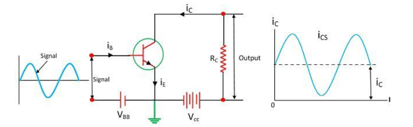
The input signal in a CE amplifier will be applied to the emitter and base terminals, while the amplified output will be taken from the collector and emitter terminals. Having a small change in the base current or input leads to a large change in the collector or output current. This is due to the transistor’s amplification property.
The change in collector current flows through the load resistor, which generates a significantly amplified output voltage.
Anatomy of a Common Emitter Amplifier
A CE transistor amplifier is a combination of BJT, resistors, and capacitors, which work together to achieve amplification and stable operation. Here are the main components:
Bipolar Junction Transistor (BJT)
This is the core amplifying element. It allows a small base current to control a larger collector current. The result is a significant output.
Biasing Resistors
Such resistance is used to set the DC operating point (Q-point) of the transistor. This ensures it operates in the active regions, where distortion is minimal. This is typically used in a voltage divider bias configuration.
Collector Resistor
The resistor is connected to the collector leg. It develops the output voltage and also limits the collector current. This voltage gain is directly proportional to its value.
Emitter Resistor
This one provides thermal stability and negative DC feedback, both of which are vital for stabilizing the Q-point. It can also be used to control the gain if left unbypassed.
Input Coupling Capacitor
This capacitor connects the input AC signal source to the transistor’s base. It also blocks any DC component from the signal source, preventing interference with the amplifier’s DC bias conditions.
Output Coupling Capacitors
It connects the output to the load or the next amplifier stage. It also blocks the DC component of the output. This allows only the amplified AC signal to pass.
Emitter Bypass Capacitor
It is connected in parallel with the emitter resistor. For AC signals, it acts as a short circuit, allowing the AC current to bypass the emitter resistor to ground and increasing the AC voltage gain of the amplifier.
DC Power Supply
Provides the necessary DC operating voltages and currents you use to bias the transistor correctly.
Biasing Techniques in CE Amplifiers
Biasing techniques are important to ensure that the common emitter amplifier is working correctly and produces an undistorted output signal. Here are the primary biasing methods in CE amplifiers.
Fixed Bias (Base Resistor Bias)
This is the simplest method of biasing for a CE amplifier. It includes using a single resistor connected from the power supply to the base of the transistor.
As you can see, it is a simple circuit with few components, which makes it cost-effective. Also, the Q-point is easy to get, as you can adjust the value of the resistor to get it.
The downside is that it comes with poor thermal stability. The collector current is highly dependent on the transistor’s gain, which varies significantly with temperature.
Collector Feedback Bias
In this configuration, the base resistor is connected to the collector terminal rather than the fixed power supply. This leads to a negative DC feedback.
Expect better stability than with the fixed bias due to negative feedback. An increase in collector current lowers the collector voltage, thereby reducing the base current. This counteracts the initial increase in collector current.
Having negative feedback has downsides, such as reducing the amplifier’s overall AC voltage gain. The stability will not be as good as the voltage divider method.
Voltage Divider Bias
This is a widely used and stable biasing method for the linear discrete circuits. In this case, a potential divider network with two resistors is used across the power supply. The aim is to provide a constant and steady voltage to the base. An emitter resistor can also be included to enhance stability.
The benefits of this biasing technique are ending up with excellent stability. The Q-point is almost independent of the transistor variations and temperature changes. Also, it allows for predictable, stable operation across different transistors of the same type.
The main downside is that it requires more components than the other two methods. Also, some AC voltage gain can be sacrificed if the emitter resistor is not entirely bypassed.
Characteristics and Performance Metrics of the CE Amplifier
Signal inversion: This is a key characteristic of the common emitter amplifier. The output signal will always be 180 degrees out of phase compared to the input signal. A positive half-cycle input results in a negative half-cycle output and vice versa.
Active region operation: The transistor must be biased to operate strictly within the active region for you to get undistorted amplification. You can achieve this through biasing circuits, such as a voltage divider bias.
Temperature sensitivity: Transistor parameters such as the base-emitter voltage and current gain are sensitive to temperature changes. Without proper biasing and stabilization, performance will generally drift, leading to instability and distortion.
Frequency response: The amplifier gain is relatively constant over the mid-frequency range, but drops off at low and high frequencies.
Bandwidth: The frequency range between the lower and upper cut-off frequencies determines the amplifier’s bandwidth.
Here is a table highlighting the key performance metrics
| Parameter | Characteristic | Typical Value |
| Voltage gain | Medium to high | 100 |
| Current gain | High | 50 – 200 |
| Power gain | High | Product of current and voltage gains |
| Input impedance | Medium | ~1 kΩ |
| Output impedance | Medium to high | ~10 kΩ or less |
| Phase shift | Inverted | 180 degrees |
Applications of the Common Emitter Amplifier
The CE amplifier does have many applications. Below is a list of the most common applications.
- Audio frequency amplification in audio systems is used to amplify low-level signals from sources such as magnetic tape heads or microphones. Examples include public address systems, stereo amplifiers and receivers, and headphone amplifiers.
- Radio frequency circuits could also use this type of amplifier for communication systems. This is for signal amplification, tuned amplifiers, low-noise amplifiers, and more.
- Digital switching applications, such as logic circuits and driving loads
- Building complex circuits, such as working with operational amplifiers and cascaded amplifiers.
Frequency Response of the CE Amplifier
The frequency response of a common emitter amplifier describes how the voltage gain changes with the frequency of the input signal. Ideally, an amplifier should have a constant gain across all frequencies, but that is not the case in practice. Having capacitors in the circuit makes the gain drop off at very high and very low frequencies.
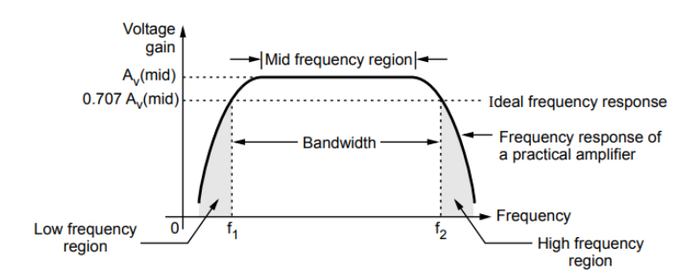
The frequency response is best visualized in a Bode plot, where the gain in decibels (DB) is plotted against frequency on a logarithmic scale. The resulting curve has three main regions: the low-frequency region, the midband region, and the high-frequency region.
Low Frequency Region
At low frequencies, the amplifier’s gain decreases as there is an increase in reactance of the external coupling and bypass capacitors.
There is a lower cutoff frequency as well. This is the frequency at which the overall voltage drops to 70.7% of its maximum midband value.
Midband Frequency Region
In the midband frequency range, the reactance of the external coupling and bypass capacitors is negligible. Also, the internal transistor capacitances have very high reactance.
In this region, you should expect constant gain. The amplifier provides its maximum and most stable voltage gain, which is mostly flat.
The AC analysis of the amplifier typically assumes operation in the midband range.
High Frequency Region
The gain drops again at high frequencies. This is primarily due to the internal parasitic capacities of the BJT and the stray wiring capacitance.
The main internal capacitances come from the base-emitter capacitance and the collector-base capacitance.
The collector-base capacitance is another problem of the CE amplifier due to the Miller effect. Because of the 180-degree phase inversion, this capacitance appears much larger at the input. This creates a low-pass filter that shunts the high-frequency signal to ground. The result is a reduction of the input resistance and overall gain.
Common Problems, Troubleshooting & Repair of the CE Amplifier
The common emitter amplifier might have a few problems that make it harder for it to work. Here is what you can expect as a problem with its likely cause.
| Problem | Symptom | Likely Issue |
| No output signal | There is no sound/signal, even with the presence of an input | No power supply Open capacitor Faulty transistorShort circuit in the wiring |
| Distorted output | Signal is clipped, fuzzy, or unclear | Incorrect DC biasing The input signal is too largeMissing emitter bypass capacitor |
| Low gain | The output signal is weak, or it is not larger than the input signal. | Emitter bypass capacitor is open or has the wrong valueIncorrect resistor valuesFaulty transistor |
| Hum or Buzz sound | Unwanted noise in the audio output | Power supply filtering Ground loopsThere are loose connections or poor shielding |
| Overheatng | Transistors or resistors tend to become excessively hot | Thermal runawayThe Q-point set for a very high current Short circuit Incorrect component values |
Conclusion
The Common Emitter amplifier is a fundamental building block of many analog electronics. It is defined by its emitter terminal being the common to both the input and output circuits. It is highly valued for its ability to provide significant gains in both current and voltage. This results in a higher power gain than other basic BJT amplifier types.
Please send RFQ , we will respond immediately.
Frequently Asked Questions
Why is the common emitter configuration a popular choice?
The CE amplifier is popular because it offers a high voltage gain, decent current gain, and good overall amplification performance. Also, it offers flexible design options, which means great flexibility.
What is the Q-point in the common emitter amplifier?
The Q-point or quiescent point is the DC operating point of a transistor. It determines how the amplifier behaves for AC signals. This point ensures maximum undistorted output swing, stable gain, and reduced distortion due to saturation or cut-off.
Why is biasing important in CE amplifiers?
Biasing is vital for setting the transistor’s DC currents and voltages vital to keep it in the active region. Without biasing, the amplifier may end up distorting the signal or fail to amplify correctly.


