
SN74LVC1G08DBVR datasheet | SOT23-5
- Logic Type: AND Gate
- Number of Circuits: 1
- Number of Inputs: 2
- Package: SOT-23-5


FREE delivery for orders over HK$250.00

Quick response, quick quotaton

Flash shipment,no worries after sales

Original channel,guarantee of the authentic products
Electronics: voltage shifting from 3.3V to 1.65V with SN74LVC
SN74LVC1G08DBVR
The SN74LVC1G08DBVR is a compact 2-input AND gate IC that’s perfect for digital circuits. It runs on a supply voltage from 1.65V to 5.5V, so it’s flexible for many applications. Thanks to its fast switching (around 3.6ns at 3.3V), it works well in high-speed systems. It’s also energy-efficient, with low power consumption both when it’s idle and active. Plus, it can handle temperatures from -40°C to +125°C, making it reliable in tough industrial or automotive environments. The output drive is strong, so it connects easily with other logic devices. Its small DBVR package makes it ideal for tight spaces. This logic gate is great for signal processing and embedded systems where speed and low power are key.
SN74LVC1G08DBVR Pinout Diagram
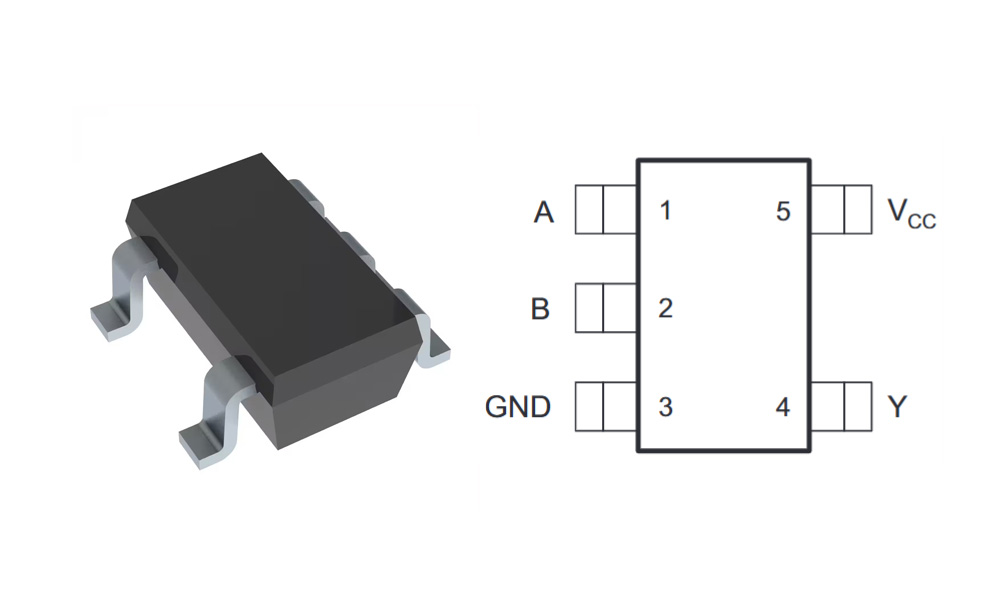
| Pin Number | Pin Name | Function |
|---|---|---|
| 1 | A | Input (First input of the AND gate) |
| 2 | B | Input (Second input of the AND gate) |
| 3 | Y | Output (Result of the AND operation) |
| 4 | GND | Ground |
| 5 | VCC | Power supply (1.65V to 5.5V) |
For the SN74LVC1G08DBVR, here’s a quick rundown of the pinout:
-
A and B (Pins 1 and 2): These are the inputs for the AND gate. Both need to be connected to logic signals. The output, Y, will only be high (1) if both inputs are high (1).
-
Y (Pin 3): This is the output. It shows the result of the AND operation. Make sure to connect it properly to handle downstream logic signals.
-
VCC (Pin 5): This is where you connect the power supply. Use a voltage between 1.65V and 5.5V for the best performance.
-
GND (Pin 4): Connect this pin to the ground.
A couple of things to remember:
-
Make sure your voltage levels are within the 1.65V to 5.5V range.
-
Place a decoupling capacitor (like 0.1µF) near VCC to help reduce noise.
-
The Y output depends on both inputs being high—if either input is low, the output will be low.
SN74LVC1G08DBVR Equivalent Logic Gate
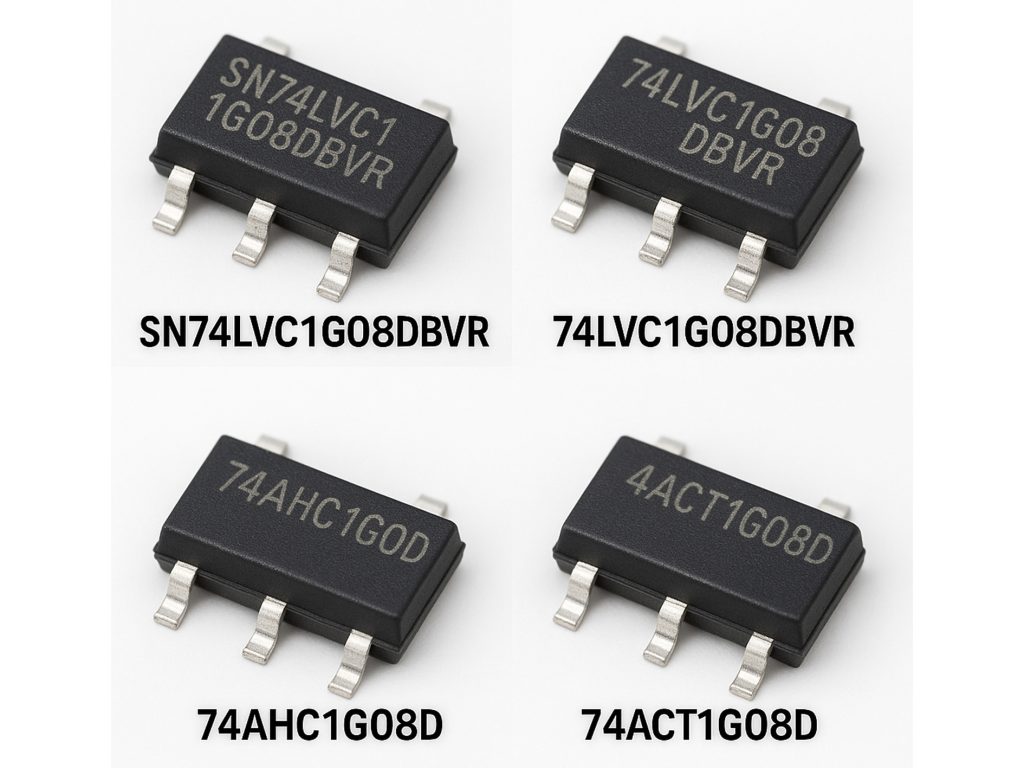
| Parameter | SN74LVC1G08DBVR | 74LVC1G08DBVR | 74AHC1G08D | 74ACT1G08D |
|---|---|---|---|---|
| Package Type | SOT-23 | SOT-23 | SOT-23 | SOT-23 |
| Input Voltage | 1.65V – 5.5V | 1.65V – 5.5V | 2V – 5.5V | 4.5V – 5.5V |
| Output Voltage | 0 to VCC | 0 to VCC | 0 to VCC | 0 to VCC |
| Logic Family | LVC (Low Voltage CMOS) | LVC (Low Voltage CMOS) | AHC (Advanced CMOS) | ACT (Advanced CMOS) |
| Propagation Delay | 3.5 ns | 3.5 ns | 7 ns | 5 ns |
| Features | Low power, high-speed | Similar functionality | Higher speed, less power efficient | Higher current drive, faster speed |
When looking at the SN74LVC1G08DBVR and 74LVC1G08DBVR, they’re pretty much the same in terms of features and performance, so you can easily swap them out for each other.
If you need something faster, the 74AHC1G08D could be a good choice—it’s quicker, but it does use more power, so it’s better for high-speed projects, not low-power ones.
The 74ACT1G08D is another option if you need more current drive and even faster speeds. It works great for high-load, high-speed needs, but keep in mind that it’ll draw more power.
SN74LVC1G08DBVR AND Gate Circuit Example
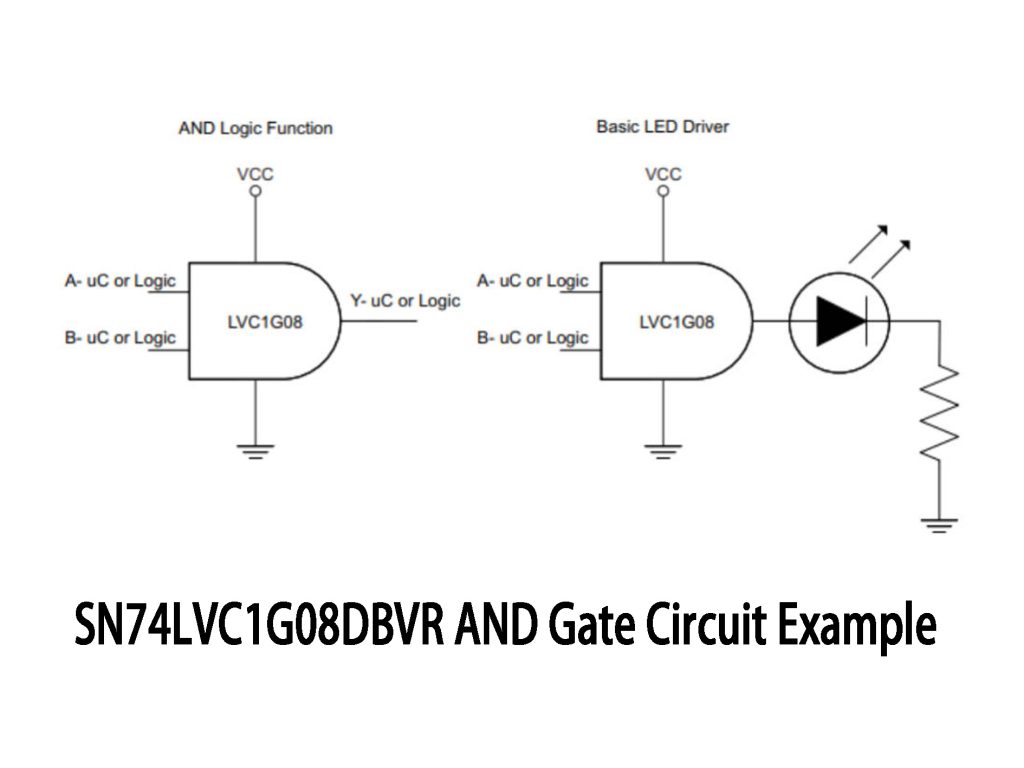
The image shows an example of how the SN74LVC1G08DBVR works in a circuit.
On the left, we have the basic AND gate function. The inputs (A and B) are logic signals or microcontroller outputs. When both inputs are HIGH (1), the output (Y) is HIGH. If either input is LOW (0), the output will be LOW. This is the core functionality of an AND gate.
On the right, the AND gate is used to drive an LED. The LED only lights up when both inputs (A and B) are HIGH, and there’s a current-limiting resistor to protect the LED. This shows how an AND gate can be used in simple control circuits, like turning on an LED based on specific conditions.
SN74LVC1G08DBVR Input Voltage Levels
The SN74LVC1G08DBVR is part of the LVC (Low-Voltage CMOS) family, which means it works well at low voltage levels while keeping logic integrity intact.
For input voltage levels:
-
High-Level Input Voltage (VIH): At 3.3V (Vcc), the minimum is 2V. For a 5V supply, it’s around 3.5V.
-
Low-Level Input Voltage (VIL): At 3.3V (Vcc), the maximum is 0.8V. With a 5V supply, it’s around 1.5V.
These voltage levels ensure the gate switches correctly and recognizes high or low input signals. The device can handle various logic families, making it ideal for low-power designs.
SN74LVC1G08DBVR SMD Logic Application
The SN74LVC1G08DBVR is often used in microcontroller interfacing and control logic circuits.
In microcontroller interfacing, it’s handy for combining multiple signals to perform an AND operation. For example, you could use it to check that certain conditions are met before triggering an output, making it perfect for signal conditioning.
In control logic circuits, the IC is used to enable or disable actions based on multiple input conditions. A great example is motor control—if both conditions are true, like power being on and a switch closed, the motor gets activated.
These two applications showcase how versatile and useful the SN74LVC1G08DBVR can be in real-world circuits.
SN74LVC1G08DBVR Arduino Digital Logic Interface
You can easily use the SN74LVC1G08DBVR with an Arduino to perform an AND gate operation. Here’s how:
-
Inputs: Connect two Arduino digital pins to the inputs of the SN74LVC1G08DBVR (A and B). For example, use pin 2 for A and pin 3 for B.
-
VCC and Ground: Connect the VCC pin to the 5V pin on the Arduino and the GND pin to the Arduino’s GND.
-
Output: The Y output pin from the gate will give you the AND result. You can connect this to an LED or another component, using a current-limiting resistor.
This setup lets you control devices like LEDs based on the AND operation of the two inputs, making it perfect for simple logic tasks like conditional control.
More Like This

MC5430F
Motorola

JD54LS51BCA
National Semiconductor

USPLSI2032VE-110LB49
Lattice Semiconductor Corporation
74S22PC
Rochester Electronics, LLC

9504DC
National Semiconductor

9005PC
National Semiconductor

9007DC
National Semiconductor
9004DC
National Semiconductor

SN74HC804DWR
Texas Instruments
SN700863DWR
Texas Instruments
4001BDMQB
National Semiconductor
54F02FMQB
National Semiconductor
Also Add to Cart

8N4SV76KC-0090CDI8
Renesas Electronics America Inc

AD620ARZ-REEL7
Analog Devices Inc.

74AHCT14PW/C1118
NXP USA Inc.
MAX3658AE/D
Analog Devices Inc./Maxim Integrated
MIC3975-2.5BMMTS
Micrel Inc.

LM2502SMX/NOPB
Texas Instruments

MAX4313EUA
Analog Devices Inc./Maxim Integrated

74ACQ245SC
Fairchild Semiconductor
XC9142C52D0R-G
Torex Semiconductor Ltd

8N4SV76FC-0055CDI8
Renesas Electronics America Inc

S-80836CLUA-B6VT2G
ABLIC Inc.

SY100E111LJG TR
Microchip Technology
Related Products
MC5430F
Motorola
JD54LS51BCA
National Semiconductor
USPLSI2032VE-110LB49
Lattice Semiconductor Corporation
74S22PC
Rochester Electronics, LLC
9504DC
National Semiconductor
9005PC
National Semiconductor
9007DC
National Semiconductor
9004DC
National Semiconductor
SN74HC804DWR
Texas Instruments
SN700863DWR
Texas Instruments
4001BDMQB
National Semiconductor
54F02FMQB
National Semiconductor
DM54S20W/883
National Semiconductor

MC3129L
Motorola
4071BDM
National Semiconductor
MC9814P
Motorola
MC9825P
Motorola

74AC11000NS
Texas Instruments
MC5420L
Motorola
MC5401L
Motorola
MC5401F
Motorola
SN74H61N
Texas Instruments
MC5410F
Motorola
MC5430L
Motorola

SN74AS138N-J
Texas Instruments
CD4023BCN
Fairchild Semiconductor
4019BDC
National Semiconductor
74H40DC
National Semiconductor
5420FMQB
National Semiconductor
4025BDM
National Semiconductor
Please send RFQ , we will respond immediately.
