CD4049UBE datasheet | pedal & pinout
- Logic Type: Inverter
- Number of Circuits: 6
- Number of Inputs: 1
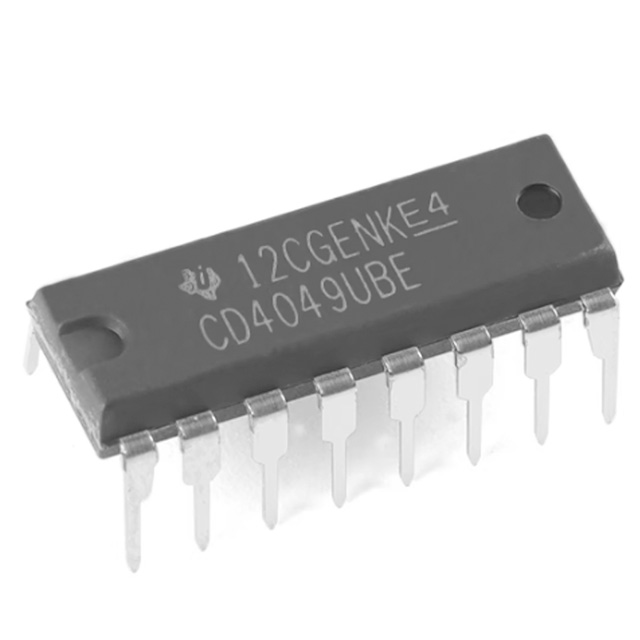
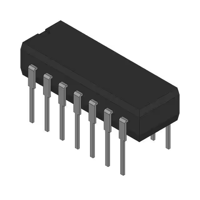
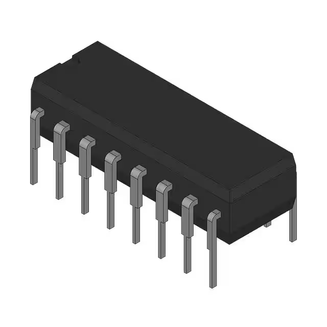
- Package: 16-PDIP

FREE delivery for orders over HK$250.00

Quick response, quick quotaton

Flash shipment,no worries after sales

Original channel,guarantee of the authentic products
CD4049UBE headphone amp – finished
CD4049UBE Pinout

The CD4049UBE is a hex inverter buffer IC designed for high-voltage CMOS applications. It contains six independent inverters with high drive capability, typically used for waveform shaping, signal inversion, and voltage level conversion. The device operates over a wide supply voltage range (3V to 15V), making it ideal for interfacing between different logic levels. Below is the detailed pinout for the 16-pin PDIP package.
| Pin | Symbol | Description |
|---|---|---|
| 1 | VCC | Supply Voltage |
| 2 | G | Input of Inverter 6 |
| 3 | A | Input of Inverter 1 |
| 4 | H | Output of Inverter 6 |
| 5 | B | Input of Inverter 2 |
| 6 | I | Output of Inverter 1 |
| 7 | C | Input of Inverter 3 |
| 8 | VSS | Ground (0V) |
| 9 | D | Output of Inverter 2 |
| 10 | J | Output of Inverter 3 |
| 11 | E | Input of Inverter 4 |
| 12 | K | Output of Inverter 4 |
| 13 | NC | No Connection |
| 14 | F | Input of Inverter 5 |
| 15 | L | Output of Inverter 5 |
| 16 | NC | No Connection |
The CD4049UBE offers a versatile solution for digital logic circuits where inversion and signal conditioning are needed. Its pin configuration supports easy integration into both TTL and CMOS designs, with multiple inputs and outputs arranged to support straightforward routing on standard PCBs.
