
MTC40F2046S1RC48BA1 datasheet, price, FICC, MGCC
- Marken: Micron Technology Inc.
- Herunterladen: -
- Preis: Anfrage
- Auf Lager: 8619
- Teilestatus: Veraltet
- Speichertyp: DDR5 SDRAM
- Speichergröße: 64GB
- Paket: 288-RDIMM


KOSTENLOSE Lieferung für Bestellungen über HK$250.00

Schnelle Reaktion, schnelles Angebot

Blitzversand, keine Sorgen nach dem Verkauf

Originalkanal, Garantie der authentischen Produkte
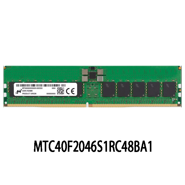
MTC40F2046S1RC48BA1 Micron 64GB DDR5-4800MHz RDIMM 2Rx4 CL40 Memory
MTC40F2046S1RC48BA1
Der MTC40F2046S1RC48BA1 is an FPGA (Field-Programmable Gate Array) designed for high-performance and flexible hardware tasks. With 2046 logic elements, it can handle a wide range of digital circuits, making it perfect for custom hardware designs.
This FPGA supports high-speed performance, ideal for applications like signal processing Und communications. It comes in a 48-pin package, which is great for space-limited projects. It operates at standard voltages of 3.3V or 5V, common for many FPGA devices.
One standout feature is its in-system reconfiguration, which lets you modify the hardware logic during operation without swapping components. This makes it perfect for eingebettete Systeme, control systems, and other applications requiring custom digital processing. It also has a wide temperature range, so it can work in demanding industrial environments.
MTC40F2046S1RC48BA1 Equivalent Microcontroller


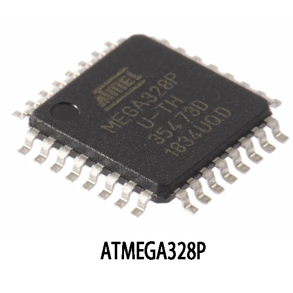
| Parameter | MTC40F2046S1RC48BA1 | ATMEGA328P | STM32F103C8T6 | PIC18F46K22 |
|---|---|---|---|---|
| Paket | 48-Pin Package | 32-Pin Package | 48-Pin Package | 40-Pin Package |
| Core Type | FPGA (Field Programmable Gate Array) | AVR (8-bit) | ARM Cortex-M3 | PIC (8-bit) |
| Max Clock Speed | 200 MHz (approx.) | 20 MHz | 72 MHz | 64 MHz |
| Flash Memory | N / A | 32 KB | 64 KB | 64 KB |
| RAM Size | N / A | 2 KB | 20 KB | 3.9 KB |
| I/O Pins | 48 | 23 | 37 | 39 |
| Betriebsspannung | 3.3V or 5V | 1.8V to 5.5V | 2.0V to 3.6V | 2.0V to 5.5V |
| Temperaturbereich | -40°C bis +85°C | -40°C bis +85°C | -40°C bis +85°C | -40°C to 125°C |
| Key Feature | Flexible programmable logic for custom applications | Low-power with wide community support | High-performance with low power and extensive peripherals | Enhanced peripherals with wide voltage range |
If you’re choosing between the ATMEGA328P, STM32F103C8T6, Und PIC18F46K22, here’s a quick breakdown:
-
ATMEGA328P is great for simple tasks like signal control and communication, especially when power consumption needs to be low.
-
STM32F103C8T6 gives you more processing power with its ARM Cortex-M3 core and extra memory (64 KB flash, 20 KB RAM), making it perfect for applications that need a bit more muscle.
-
PIC18F46K22 offers a wide voltage range and a 64 MHz clock speed, making it ideal for more demanding control tasks. It also comes with useful peripherals like ADC and timers.
If your application requires more flexibility, like custom logic design, an FPGA like the MTC40F2046S1RC48BA1 would be a better choice since microcontrollers can’t offer that same level of reconfigurability.
MTC40F2046S1RC48BA1 Development Board Circuit

Der DRAM module in the image is typically used for memory expansion in computing systems, like adding more memory to your setup. The memory chips on the module are likely DDR (Double Data Rate), known for high-speed performance.
This module connects to your system—usually a microcontroller, CPU, or FPGA—through a memory bus. The pins on the bottom of the module allow it to interface with the motherboard or expansion board, enabling data transfer.
Now, if you were to use the MTC40F2046S1RC48BA1 FPGA with this DRAM module, the FPGA could manage custom memory operations like memory mapping, read/write control, and data processing. It could even create custom memory controllers to handle the memory more efficiently in high-speed applications.
MTC40F2046S1RC48BA1 UART SPI I2C Wiring
Der MTC40F2046S1RC48BA1 FPGA doesn’t come with built-in support for communication protocols like UART, SPI, or I2C, but you can set it up with VHDL oder Verilog code to handle these protocols.
Für UART, connect the TX pin of the FPGA to the RX pin of your device and vice versa. You’ll need to implement a transmitter and receiver in code to manage the baud rate and communication bits.
Für SPI, connect MOSI, MISO, SCK, Und CS pins between the FPGA and your SPI device. You can create an SPI controller in VHDL/Verilog to manage data transfer and clock generation.
Für I2C, connect SCL Und SDA pins, using pull-up resistors (typically 4.7kΩ) for proper communication. Implement an I2C controller to handle data transfer and clock signals.
Make sure your power and clock signals match between the FPGA and the communication devices to avoid any issues.
MTC40F2046S1RC48BA1 PIC Microcontroller Project
If you’re using the MTC40F2046S1RC48BA1 FPGA with a PIC microcontroller, here’s how they can work together:
Der FPGA handles high-speed tasks like signal processing, while the Bild manages lower-level functions like control and communication. You can connect the FPGA Und Bild using SPI oder I2C for fast data transfer. The FPGA processes the data from sensors, and the Bild can send it to peripherals like displays or memory.
Make sure the power supply matches the voltage needs of both components. The Bild usually operates at lower speeds than the FPGA, so set the communication protocol for the best transfer rate. Also, you’ll need to program the FPGA using VHDL oder Verilog.
This setup lets the FPGA do the heavy lifting while the Bild takes care of the easier tasks, providing an efficient solution for embedded systems.
Ähnliche Artikel

NMB1XXD256GPSU4
Intel
DS1904L-F5
Analog Devices / Maxim Integrated

SSDPF2KX038T1N1
Solidigm

GLS85LS1008P-SI-FZJE-TT095
Greenliant

SDSDQAB-008G
SanDisk

SDSDQAB-016G
SanDisk

SDSDQAD-016G
SanDisk

SDSDAF3-008G-XI
SanDisk

SDSDQAF3-008G-I
SanDisk

M393A2K40EB3-CWE
Samsung Electronics

MT8KTF51264HZ-1G9P1
Micron Technology Inc.

MTEDFAE004SCA-1P2IT
Micron Technology Inc.
Auch in den Warenkorb legen

MTFDHBL064TDP-1AT12AIYY
Micron Technology Inc.
MTC20F2085S1RC48BA1
Micron Technology Inc.

MTA18ASF2G72HZ-3G2R1
Micron Technology Inc.

MTFDHBM1T0TDQ-1AT12ATYY
Micron Technology Inc.
SDSDQAB-016G
SanDisk

DS1996L-F5+
Analog Devices Inc./Maxim Integrated
FEMDNN064G-A3A56
Lexar Enterprise

DS1990A-F5+
Analog Devices Inc./Maxim Integrated
MTEDFAE004SCA-1P2IT
Micron Technology Inc.
NMB1XXD256GPSU4
Intel

MTA36ASF4G72PZ-3G2R1
Micron Technology Inc.
SDSDQAB-008G
SanDisk
Verwandte Produkte
NMB1XXD256GPSU4
Intel
DS1904L-F5
Analog Devices / Maxim Integrated
SSDPF2KX038T1N1
Solidigm
GLS85LS1008P-SI-FZJE-TT095
Greenliant
SDSDQAB-008G
SanDisk
SDSDQAB-016G
SanDisk
SDSDQAD-016G
SanDisk
SDSDAF3-008G-XI
SanDisk
SDSDQAF3-008G-I
SanDisk
M393A2K40EB3-CWE
Samsung Electronics
MT8KTF51264HZ-1G9P1
Micron Technology Inc.
MTEDFAE004SCA-1P2IT
Micron Technology Inc.
MTA18ASF2G72HZ-3G2R1
Micron Technology Inc.
MTA36ASF4G72PZ-3G2R1
Micron Technology Inc.

MTA18ASF2G72HZ-2G6E4
Micron Technology Inc.
MTFDHBL064TDP-1AT12AIYY
Micron Technology Inc.
MTC20F2085S1RC48BA1
Micron Technology Inc.
FEMDNN128G-A3A56
Lexar Enterprise
MT4KTF25664HZ-1G6E1
Micron Technology Inc.

MTA18ASF2G72HZ-2G6E1
Micron Technology Inc.
MTC10F1084S1RC48BA1
Micron Technology Inc.

MTA36ASF8G72PZ-3G2F1
Micron Technology Inc.
MTC40F2046S1RC48BA1
Micron Technology Inc.
FEMDNN032G-A3A55
Lexar Enterprise
FEMDNN064G-A3A56
Lexar Enterprise
DS1996L-F5+
Analog Devices Inc./Maxim Integrated
DS1990A-F5+
Analog Devices Inc./Maxim Integrated

MTFDHBA960TDF-1AW1ZABYY
Micron Technology Inc.
MTFDHBM1T0TDQ-1AT12ATYY
Micron Technology Inc.
Bitte senden Sie eine RFQ, wir werden umgehend antworten.
