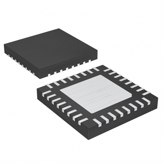
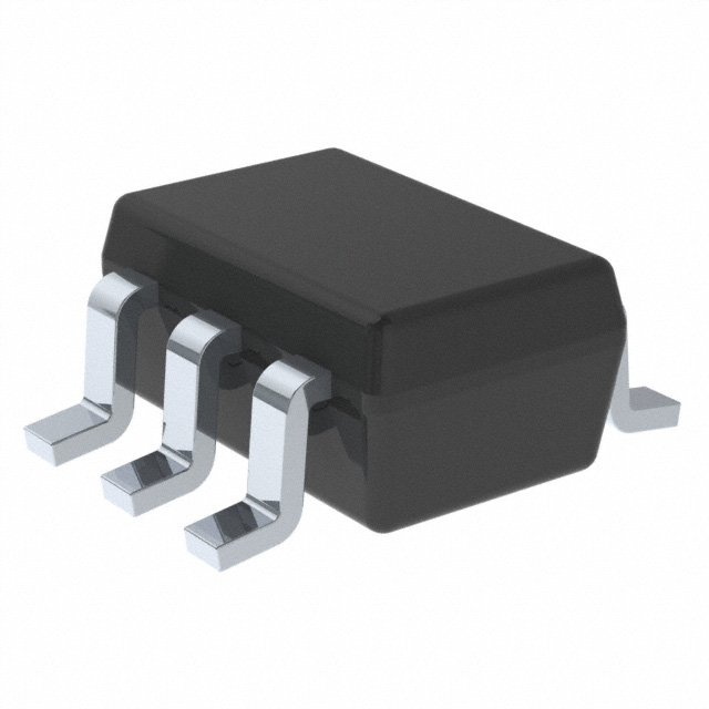
STM32F030C8T6 Datenblatt, Pinbelegung und Referenzhandbuch
- Marken: STMicroelectronics
- Herunterladen: STM32F030C8T6 Datasheet PDF
- Preis: Anfrage
- Auf Lager: 15,940
- Kernprozessor: ARM® Cortex®-M0
- Kerngröße: 32-Bit-Einzelkern
- Peripheriegeräte: DMA, POR, PWM, WDT
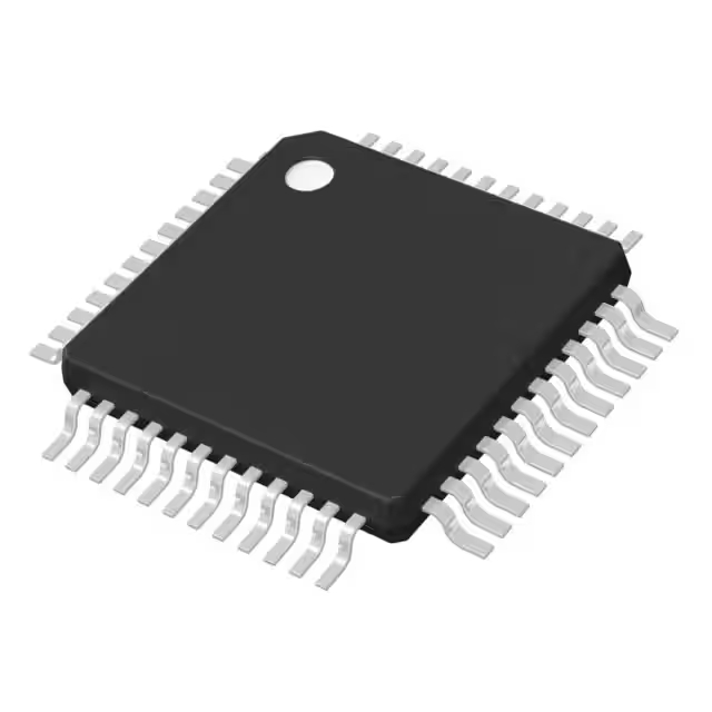
- Paket: 48-LQFP

KOSTENLOSE Lieferung für Bestellungen über HK$250.00

Schnelle Reaktion, schnelles Angebot

Blitzversand, keine Sorgen nach dem Verkauf

Originalkanal, Garantie der authentischen Produkte
STM32F030C8T6 Pinout

1:Overview of the STM32F030C8T6:
The STM32F030C8T6 is a commonly used microcontroller chip featuring an ARM Cortex-M0 core, widely applied in industrial control. It is primarily utilized in applications requiring low cost and low power consumption.
The STM32F030C8T6 operates at a maximum frequency of 48MHz and features 64KB of flash memory and 8KB of SRAM.
The operating voltage range of the STM32F030C8T6 is 2.0 to 3.6 volts, and it comes in an LQFP48 package.
The STM32F030C8T6 offers a wealth of peripheral resources, including multiple timers for various applications. With support for communication interfaces such as USART, SPI, and I²C, the controller is compatible with a wide range of external devices.
The main advantage of the STM32F030C8T6 is its low cost, making it suitable for products with limited budgets. Therefore, it is often used in consumer electronics such as smart bracelets and toys, as well as in industrial control applications like simple control devices.
2:Table of pin function replacement for STM32F030C8T6:
Table 1
| Pin name | AF0 | AF1 | AF2 | AF3 | AF4 | AF5 | AF6 |
|---|---|---|---|---|---|---|---|
| PA0 | – | USART1_CTS(1) USART2_CTS(2)(3) |
– | – | USART4_TX(2) | – | – |
| PA1 | EVENTOUT | USART1_RTS(1) USART2_RTS(2)(3) |
– | – | USART4_RX(2) | TIM15_CH1N(2) | – |
| PA2 | TIM15_CH1(2)(3) | USART1_TX(1) USART2_TX(2)(3) |
– | – | – | – | – |
| PA3 | TIM15_CH2(2)(3) | USART1_RX(1) USART2_RX(2)(3) |
– | – | – | – | – |
| PA4 | SPI1_NSS | USART1_CK(1) USART2_CK(2)(3) |
– | – | TIM14_CH1 | USART6_TX(2) | – |
| PA5 | SPI1_SCK | – | – | – | – | USART6_RX(2) | – |
| PA6 | SPI1_MISO | TIM3_CH1 | TIM1_BKIN | – | USART3_CTS(2) | TIM16_CH1 | EVENTOUT |
| PA7 | SPI1_MOSI | TIM3_CH2 | TIM1_CH1N | – | TIM14_CH1 | TIM17_CH1 | EVENTOUT |
| PA8 | MCO | USART1_CK(1) | TIM1_CH1 | EVENTOUT | – | – | – |
| PA9 | TIM15_BKIN(2)(3) | USART1_TX | TIM1_CH2 | – | I2C1_SCL(1)(2) | MCO(2) | – |
| PA10 | TIM17_BKIN | USART1_RX | TIM1_CH3 | – | I2C1_SDA(1)(2) | – | – |
| PA11 | EVENTOUT | USART1_CTS | TIM1_CH4 | – | – | I2C_SCL | – |
| PA12 | EVENTOUT | USART1_RTS | TIM1_ETR | – | – | I2C_SDA | – |
| PA13 | SWDIO | IR_OUT | – | – | – | – | – |
| PA14 | SWCLK | USART1_TX(1), USART2_TX(2)(3) | – | – | – | – | – |
| PA15 | SPI1_NSS | USART1_RX(1), USART2_RX(2)(3) | – | EVENTOUT | USART4_RTS(2) | – | – |
Table 2
| Pin name | AF0 | AF1 | AF2 | AF3 | AF4 | AF5 |
|---|---|---|---|---|---|---|
| PB0 | EVENTOUT | TIM3_CH3 | TIM1_CH2N | – | USART3_CK(1) | – |
| PB1 | TIM14_CH1 | TIM3_CH4 | TIM1_CH3N | – | USART3_RTS(1) | – |
| PB2 | – | – | – | – | – | – |
| PB3 | SPI1_SCK | EVENTOUT | – | – | USART5_TX(1) | – |
| PB4 | SPI1_MISO | TIM3_CH1 | EVENTOUT | – | USART5_RX(1) | TIM17_BKIN(1) |
| PB5 | SPI1_MOSI | TIM3_CH2 | TIM16_BKIN | I2C1_SMBA | USART5_CK_RTS(1) | – |
| PB6 | USART1_TX | I2C1_SCL | TIM16_CH1N | – | – | – |
| PB7 | USART1_RX | I2C1_SDA | TIM17_CH1N | – | USART4_CTS(1) | – |
| PB8 | – | I2C1_SCL | TIM16_CH1 | – | – | – |
| PB9 | IR_OUT | I2C1_SDA | TIM17_CH1 | EVENTOUT | – | SPI2_NSS(1) |
| PB10 | – | I2C2_SCL(2) | – | – | USART3_TX(1) | SPI2_SCK(1) |
| PB11 | EVENTOUT | I2C2_SDA(2) | – | – | USART3_RX(1) | – |
| PB12 | SPI1_NSS(1/3) | EVENTOUT | TIM1_BKIN | – | USART3_RTS(1) | TIM15(1) |
| PB13 | SPI1_SCK(2) | – | TIM1_CH1N | – | USART3_CTS(1) | I2C2_SCL(1) |
| PB14 | SPI1_MISO(2) | TIM15_CH1(1/3) | TIM1_CH2 | – | USART3_RTS(1) | I2C2_SDA(1) |
| PB15 | SPI1_MOSI(2) | TIM15_CH2(1/3) | TIM1_CH3 | TIM15_CH1N(1/3) | – | – |
Table 3. Alternate functions selected through GPIOC_AFR registers for port C
| Pin name | AF0(1) | AF1(1) | AF2(1) |
|---|---|---|---|
| PC0 | EVENTOUT(1) | – | USART6_TX(1) |
| PC1 | EVENTOUT(1) | – | USART6_RX(1) |
| PC2 | EVENTOUT(1) | SPI2_MISO(1) | – |
| PC3 | – | SPI2_MOSI(1) | – |
| PC4 | EVENTOUT(1) | USART3_TX(1) | – |
| PC5 | – | USART3_RX(1) | – |
| PC6 | TIM3_CH1(1) | – | – |
| PC7 | TIM3_CH2(1) | – | – |
| PC8 | TIM3_CH3(1) | – | – |
| PC9 | TIM3_CH4(1) | – | – |
| PC10 | USART4_TX(1) | USART3_TX(1) | – |
| PC11 | USART4_RX(1) | USART3_RX(1) | – |
| PC12 | USART4_CK(1) | USART3_CK(1) | USART5_TX(1) |
| PC13 | – | – | – |
| PC14 | – | – | – |
| PC15 | – | – | – |
1. Available on STM32F030Cx devices only.
Table 4. Alternate functions selected through GPlOD AFR registers for port D
| Pin name | AF0(1) | AF1(1) | AF2 |
|---|---|---|---|
| PD2 | TIM3_ETR(1) | USART3_RTS(1) | USART5_RX(1) |
1. Available on STM32F030xC devices only.
Table 5. Alternate functions selected through GPlOF AFR registers for port F
| Pin name | AF0 | AF1 | |
|---|---|---|---|
| PF0 | – | I2C1_SDA(1) | |
| PF1 | – | I2C1_SCL(1) |






.jpg)

