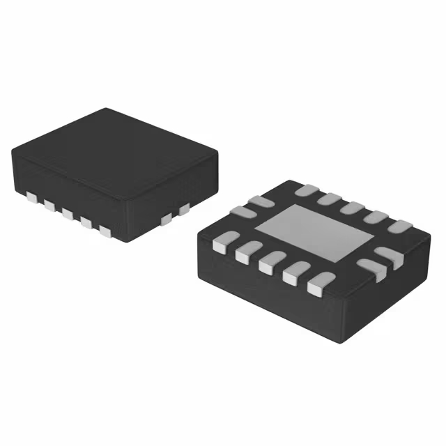
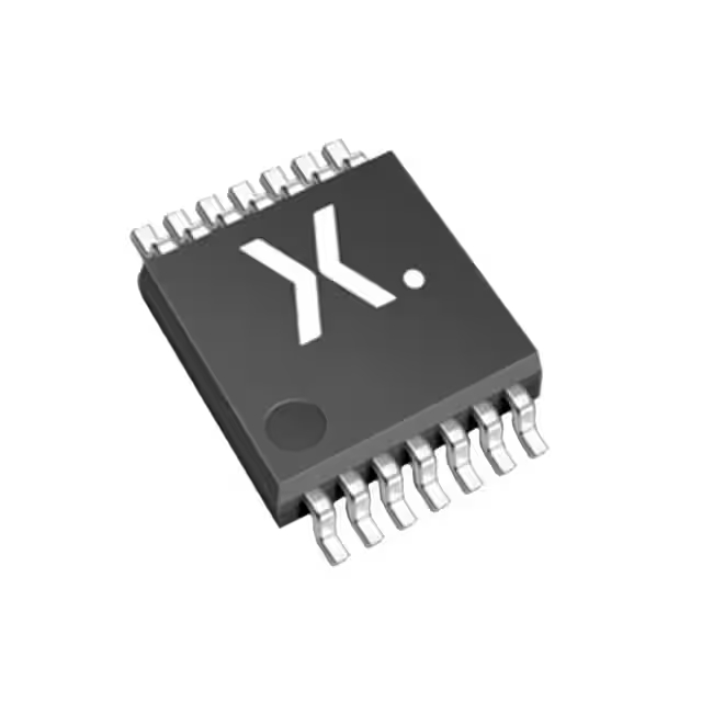
CD4069UBE Hoja de datos, distribución de pines y PDF
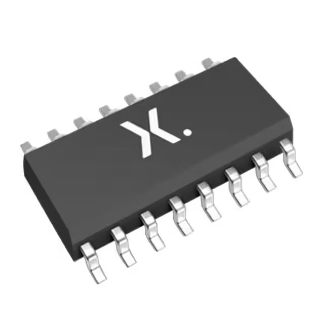
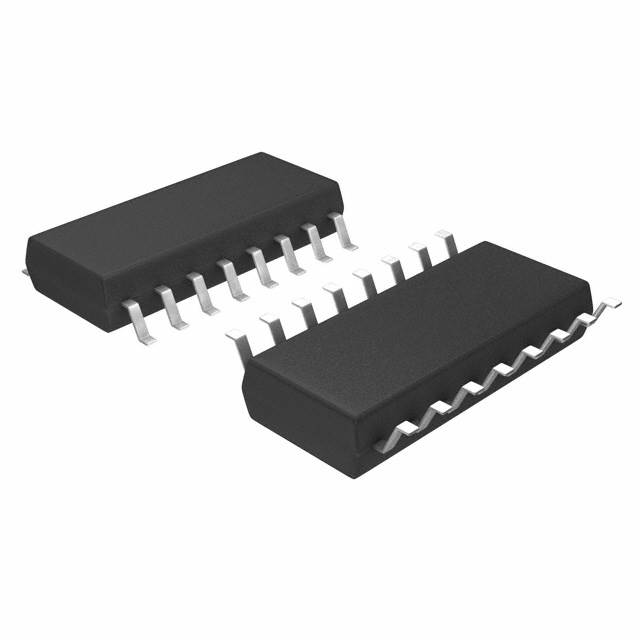
- Tipo de lógica: Inversor
- Número de circuitos: 6
- Número de entradas: 1
- Paquete: 14-PDIP

Envío GRATUITO para pedidos superiores a HK$250.00

Respuesta rápida, cotización rápida.

Envío rápido, sin preocupaciones posventa.

Canal original, garantía de los productos auténticos.
cd4069ube
The CD4069UBE is a CMOS hex inverting buffer IC that’s designed to be power-efficient. It has six independent inverters with high noise immunity, making it reliable for various applications. With a voltage range from 3V to 15V, it can handle different input levels, offering great flexibility. It’s commonly used for logic level shifting, signal inversion, and other digital circuits. Thanks to its low quiescent current, it’s perfect for low-power designs. Plus, it offers fast switching and low propagation delay for efficient signal processing.
cd4069ube pinout
| Número PIN | Nombre del pin | Función |
|---|---|---|
| 1 | 1A | Input for Inverter 1 |
| 2 | 1 año | Output for Inverter 1 |
| 3 | 2A | Input for Inverter 2 |
| 4 | 2 años | Output for Inverter 2 |
| 5 | 3A | Input for Inverter 3 |
| 6 | 3 años | Output for Inverter 3 |
| 7 | Tierra | Suelo |
| 8 | 4A | Input for Inverter 4 |
| 9 | 4 años | Output for Inverter 4 |
| 10 | 5A | Input for Inverter 5 |
| 11 | 5Y | Output for Inverter 5 |
| 12 | 6A | Input for Inverter 6 |
| 13 | 6Y | Output for Inverter 6 |
| 14 | VCC | Power Supply (3V to 15V) |
For the CD4069UBE, here’s a quick breakdown of the pins. The input pins (1A-6A) take in your signal, and the output pins (1Y-6Y) give the inverted signal. Just make sure the input voltage levels fit your circuit’s logic needs. The GND pin connects to your circuit’s common ground, so everything runs smoothly. As for VCC, this powers the IC, so it should be connected to a supply between 3V and 15V to keep it working properly.
cd4069ube equivalent
| Parámetro | CD4069UBE | MC14069UB | 74HC4069 | 74HCU4069 |
|---|---|---|---|---|
| Tipo de paquete | DIP-14 | DIP-14 | DIP-14 | DIP-14 |
| Voltaje de suministro | 3 V a 15 V | 3 V a 18 V | 2 V a 6 V | 2 V a 6 V |
| Corriente máxima de salida | 8 mA | 8 mA | 6mA | 6mA |
| Temperatura de funcionamiento | -55°C a 125°C | -40°C a 85°C | -40°C to 125°C | -40°C to 125°C |
| Notas clave | Standard hex inverting buffer IC | Direct replacement, slightly wider voltage range | Higher speed, lower voltage operation | CMOS, higher speed, lower voltage operation |
The MC14069UB is almost the same as the CD4069UBE but can handle a higher voltage (up to 18V), so it’s usually a simple replacement. The 74HC4069 and 74HCU4069 are also similar, but they operate at a lower voltage range (2V to 6V) and are typically faster, which could be great for high-frequency applications. However, they might not be ideal if you need the full voltage range of the CD4069UBE. When swapping parts, just make sure the voltage and current match what you need, and don’t forget to check the temperature range for your specific application.
cd4069ube logic gate circuit example

The circuit you’re looking at is an oscillator built with the inverters inside the CD4069UBE chip. The IC has six inverters, but only a few are used here (I1, I2, I3, etc.), with the rest left unused. R1 (680KΩ) and C1 (0.001μF) form the timing circuit, which sets the frequency of the square wave output. This simple setup creates a square wave with a frequency of 1kHz. VDD powers the circuit with a voltage between +3V to +16V, and VSS is grounded. This is an astable multivibrator that keeps switching between high and low, making it great for clock pulses or timing signals.
cd4069ube buffer amplifier usage
The CD4069UBE is mainly an inverter, but it can also work as a buffer amplifier with a bit of setup. If you use just one inverter and provide the right feedback, it can amplify the signal without changing its logical level, while handling more current. It’s great for impedance matching between circuit stages, ensuring signals don’t get weakened. It can also act as a voltage buffer, driving components that need more current than what the previous stage could provide. However, if you need high speed or more current capacity, you might want to look at other dedicated buffer ICs.
cd4069ube inverting buffer application
The CD4069UBE can be used as an inverting buffer to invert signals in your circuit. It works by taking the input signal and inverting it, so a high (1) becomes low (0) and vice versa. It’s great for driving larger loads, as it can handle more current than typical logic gates. You can also use it to shift voltage levels between different logic systems. It’s useful in oscillator circuits to generate square waves or for signal isolation, preventing interference between circuit stages. However, it’s better for low-frequency applications and might not handle high-current loads well.


