
STM32H562VGT6 Specs & Datasheet
- Velocidad: 250MHz
- Número de E/S: 80
- Procesador central: ARM® Cortex®-M33
- Paquete: 100-LQFP


Envío GRATUITO para pedidos superiores a HK$250.00

Respuesta rápida, cotización rápida.

Envío rápido, sin preocupaciones posventa.

Canal original, garantía de los productos auténticos.
STM32H562VGT6 Microcontroller Detailed Overview

The STM32H562VGT6 is part of STMicroelectronics’ advanced STM32H5 series, featuring the powerful Arm® Cortex®-M33 processor operating at speeds up to 250MHz. It is specifically designed for high-performance and security-sensitive embedded applications.
Key Features and Specifications
CPU Core: Arm® Cortex®-M33 (250MHz), featuring TrustZone® security technology
Performance Metrics:
1. CoreMark® score up to 1023 (4.092 CoreMark®/MHz)
2. Dhrystone 2.1 benchmark performance of 375 DMIPS
3. Single-precision Floating Point Unit (FPU)
Memory Specifications:
1. Flash memory: 1MB (ECC support, dual-bank independent operation)
2. SRAM total: 640KB (256KB SRAM1, 64KB ECC-enabled SRAM2, and 320KB optionally ECC-enabled SRAM3)
3. Backup SRAM: 4KB
Security Features:
1. Arm® TrustZone® for secure and non-secure code separation
2. Secure Firmware Installation (SFI) mechanism
3. Supports secure boot and firmware updates
4. Hardware cryptographic accelerators (HASH, ECDSA signature verification)
5. True Random Number Generator (TRNG, compliant with NIST SP800-90B)
6. Active tamper detection and protection
Peripheral Interfaces:
1. ADC: Two 12-bit ADCs with up to 5 Msps sampling rate
2. DAC: One 12-bit DAC with two channels
3. Extensive communication interfaces: 12 USART/UART, 6 SPI, 4 I2C, 1 I3C, 2 FDCAN, USB 2.0 Full-Speed (Host and Device), USB Type-C/PD interfaces
Power Supply Range: 1.71V to 3.6V with multiple low-power modes including Sleep, Stop, and Standby
Paquete: 100-pin LQFP (14x14mm)
Pinout Diagram
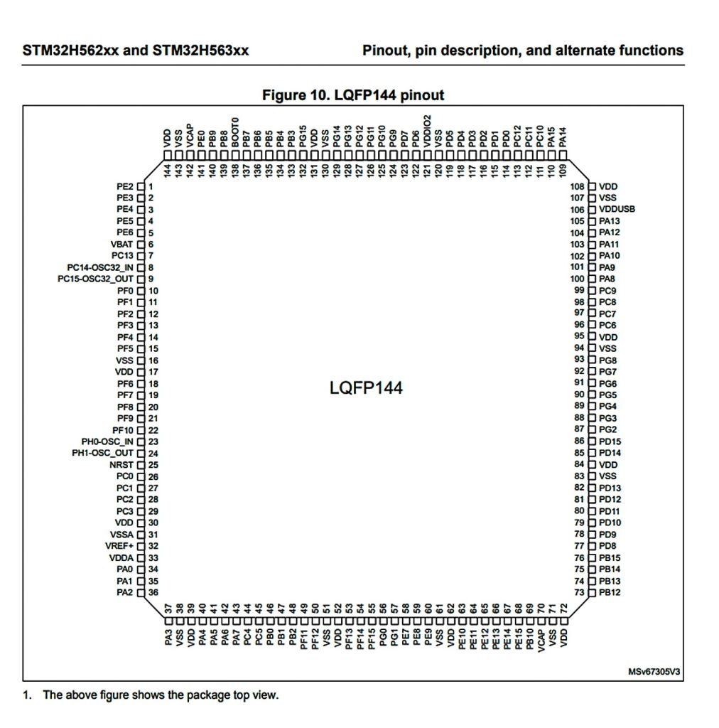
The STM32H562VGT6 comes in a 100-pin LQFP package, offering 80 general-purpose I/O pins. Key pin functionalities include:
1. Power and Ground: VDD, VSS, VDDA, VSSA
2. Debug Interface: SWD (SWCLK, SWDIO)
3. Clock Pins: External oscillator connections (OSC_IN, OSC_OUT)
4. Peripheral Pins: USART, SPI, I2C, CAN, USB, ADC/DAC analog input/output
(For the complete pin configuration, refer to the STM32H562VGT6 datasheet, Figure 10 pinout diagram)
Peripheral Circuit Design Considerations
1. Power Supply Design: Recommended low-noise LDO regulators or integrated SMPS modules provide a stable 1.8V-3.3V supply, enhancing operational reliability.
2. Clock Circuit Design: External precision crystals (8MHz-32MHz) are recommended for accurate clock generation, optimizing performance and meeting communication interface specifications.
3. Analog Circuit Design: ADC inputs should include low-pass filtering and RC buffering; DAC outputs require filtering circuits for signal integrity.
4. Debug and Programming Interface: Integrated SWD interface compatible with ST-Link or other debugging tools for firmware programming and debugging.
5. ESD and Protection Circuits: GPIOs and communication interface pins should be protected with TVS diodes or ESD protection components to enhance reliability.
The STM32H562VGT6 microcontroller delivers robust performance and high security, making it ideal for industrial control systems, consumer electronics, smart home devices, and IoT applications. Proper peripheral circuit design enables the microcontroller to leverage its full performance potential, suitable for complex application environments.
Más como esto

TPIC6C596PWG4
Texas Instruments
TPIC6C596PW
Texas Instruments

MC14557BDWR2G
onsemi

74HCT595D,112
Nexperia USA Inc.

SN74AHC594D
Texas Instruments
CD4031BPWR
Texas Instruments
CD4035BPWR
Texas Instruments
CD74HCT166M
Texas Instruments
")
TC74HC165AP(F)
Toshiba Semiconductores y almacenamiento

SN74HC595ANSR
Texas Instruments

SN74LV166ADBR
Texas Instruments

BU4015BF-E2
Semiconductor Rohm
Añadir también al carrito

XRT71D03IVTR-F
MaxLinear, Inc.

ADM3483ARZ
Dispositivos analógicos Inc.
RE46C194S16T
Tecnología de microchip

GS2970AIBE3
Corporación Semtech

SN74AS869NT
Texas Instruments

5PB1104CMG1
Renesas Electronics America Inc

LC4384B-75FTN256C
Corporación Lattice Semiconductor

LM2937IMPX-5.0
Texas Instruments

LDK320AU50R
STMicroelectrónica

LM96194CISQ/NOPB
Texas Instruments

X1227S8
Renesas Electronics America Inc

SN74S283N
Texas Instruments
Productos relacionados
TPIC6C596PWG4
Texas Instruments
TPIC6C596PW
Texas Instruments
MC14557BDWR2G
onsemi
74HCT595D,112
Nexperia USA Inc.
SN74AHC594D
Texas Instruments
CD4031BPWR
Texas Instruments
CD4035BPWR
Texas Instruments
CD74HCT166M
Texas Instruments
TC74HC165AP(F)
Toshiba Semiconductores y almacenamiento
SN74HC595ANSR
Texas Instruments
SN74LV166ADBR
Texas Instruments
BU4015BF-E2
Semiconductor Rohm
CD4094BPW
Texas Instruments
SN74LV595AQPWRQ1
Texas Instruments

SN74LV166ADGVR
Texas Instruments

CD74HC595NSR
Texas Instruments
SN74LV595ANSR
Texas Instruments
SN74LV594ADBR
Texas Instruments

SN74F299DWR
Texas Instruments
BU4021BF-E2
Semiconductor Rohm

74AHCT164BQ-Q100X
Nexperia USA Inc.
74HCT597D-Q100J
Nexperia USA Inc.
SN74LV165APWT
Texas Instruments
SN74AHCT594DBR
Texas Instruments
74HC594D-Q100,118
Nexperia USA Inc.

CD74HC195NSR
Texas Instruments

74LVC594ABQ-Q100X
Nexperia USA Inc.

74AHCT164D-Q100J
Nexperia USA Inc.

74AHCT164PW-Q100J
Nexperia USA Inc.
NPIC6C596BQ-Q100,1
Nexperia USA Inc.
Envíe RFQ, le responderemos de inmediato.
