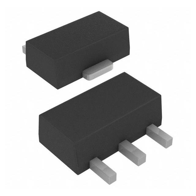
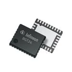
TQP3M9028 Ficha técnica, precio, PDF
- Marcas: Qorvo
- Descargar: -
- Precio: consulta
- En stock: 15009
- Frecuencia: 14MHz ~ 4GHz
- Ganar: 14.5dB
- Tipo de RF: Propósito general
- Paquete: TO-243AA

Envío GRATUITO para pedidos superiores a HK$250.00

Respuesta rápida, cotización rápida.

Envío rápido, sin preocupaciones posventa.

Canal original, garantía de los productos auténticos.
tqp3m9028
TQP3M9028 is a pretty solid broadband amplifier module covering 50 MHz to 4 GHz, easily handling VHF/UHF up to C-band. Around 1.9 GHz, you get a nice 14.7 dB gain, slightly better than spec, giving your signal a noticeable boost. Its noise stays low at around 2 dB, ensuring clear signal quality. Plus, it delivers excellent linearity with an OIP3 of +40 dBm, smoothly handling complex signals. Low power and a compact size make PCB integration easy—ideal for wireless comms and aerospace defense.
tqp3m9028 pinout and block diagram
| Número PIN | Nombre del pin | Descripción de la función |
|---|---|---|
| 1 | RF IN | RF signal input; AC coupling required |
| 2 | Tierra | Ground; ensure good grounding to avoid RF interference |
| 3 | RF OUT / VDD | RF output and power supply pin; AC coupling and external 5V bias needed |
The TQP3M9028 is a compact single-supply broadband amplifier (SOT-89-3) with plenty of integrated features. When you’re setting it up, make sure to put capacitors at both RF input and output for AC coupling, preventing DC interference. Pin 3 handles both RF output and power supply, so you’ll need an RF choke here to separate DC from RF and provide stable bias voltage. Also, solder the ground pin to a large grounding plane—it’ll cut down noise and improve heat dissipation, ensuring smoother operation.
tqp3m9028 rf amplifier circuit example

This circuit uses the TQP3M9028 amplifier. Basically, your signal enters from J1 through capacitor C2 to pin 1, isolating DC. Pin 2 just goes straight to ground for stability. Pin 3 handles both RF output and power, so you add choke L2 to separate DC from RF signals. Output then goes through capacitor C6 for AC coupling. Also, place C1 near the power line to filter high-frequency noise—use small-value capacitors like 0603 package. A large PCB ground area improves performance significantly.
tqp3m9028 50 ohm gain matching circuit

This circuit uses multiple TQP3M9028 amplifiers in parallel for higher power and linearity. Your input first passes an 18Ω resistor and 100pF capacitor, going into the first stage amplifier. Then it splits into three paths through transformers, each path driven by its own amplifier with separate 47nH chokes and matching resistors to avoid interference. Finally, two transformers merge them back into one output, maintaining a neat 50Ω match. It’s ideal for RF pre-amplification, IF stages, or boosting signal strength.
tqp3m9028 small signal lna design
Using TQP3M9028 as a small-signal LNA is actually pretty practical. Although it’s not specifically an LNA chip, it still gives decent gain (around 14.5dB), low noise (about 2dB NF), and excellent linearity (OIP3 around 40dBm) from 50MHz to 4GHz. For your circuit, put a 100pF capacitor at both input and output to block DC, a 47nH RF choke, and several bypass capacitors near the power pin. It’s perfect for wireless front-end receivers or SDR setups that need good gain and linearity without chasing ultra-low noise specs.
tqp3m9028 broadband amplifier project
If you’re looking to build a broadband RF amplifier using TQP3M9028, it’s a solid choice. It covers 50MHz to 4GHz with stable gain and excellent linearity. You can easily use it in SDR front-ends, wideband antenna buffering, or lab signal drivers. Just add a 100pF capacitor and a small resistor (like 10Ω) at the input, and a choke inductor plus decoupling capacitors at the output. Keep PCB traces short, use good grounding, and maintain 50Ω lines—you’ll get great results.
