
XCF32PVOG48C datasheet
- Brands: AMD Xilinx
- Download: -
- Price: inquiry
- In Stock: 6158
- Product Status: Obsolete
- Programmable Type: In System Programmable
- Memory Size: 32Mb
- Package: 48-TFSOP (0.724, 18.40mm Width)


FREE delivery for orders over HK$250.00

Quick response, quick quotaton

Flash shipment,no worries after sales

Original channel,guarantee of the authentic products
XCF32PVOG48C
When you’re designing with Xilinx FPGA and need a reliable solution to load configurations automatically after power-up, the XCF32PVOG48C is your best bet. With 32Mbit (4MB) capacity, it easily handles large or multiple FPGA bitstreams. It uses a standard serial PROM interface compatible with Spartan-3/6 or Virtex FPGAs, runs on a 2.5V supply, and comes in a convenient VQFP48 package. Programming via JTAG with Vivado or iMPACT is straightforward, and you’ll appreciate features like multiboot, write protection, and sector-based erasure—perfect for embedded applications.
XCF32PVOG48C Pinout
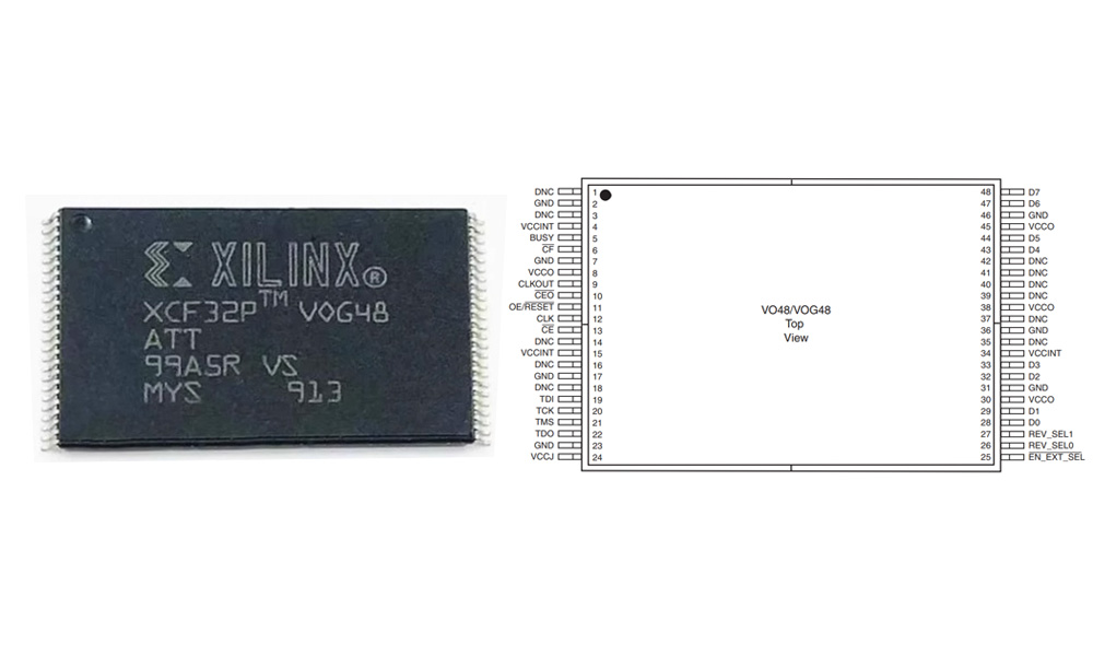
| Pin No. | Name | Type | Description |
|---|---|---|---|
| 1–8 | DQ0–DQ7 | I/O | Data lines. In serial mode, only DQ0 is used. In BPI mode, used as parallel data bus. |
| 9 | CCLK | Input | Configuration clock signal, sourced from FPGA or JTAG. |
| 10 | CEO | Output | Daisy chain output, connects to the CE pin of the next PROM. |
| 11 | CS | Input | Chip select (active low), enables the PROM. |
| 12 | OE/RESET | Input | Output enable / Reset input (active low). |
| 13 | RDY/BUSY | Output | Indicates whether the PROM is ready. |
| 14 | CLK | Input | Used in parallel mode. |
| 15 | WE | Input | Write enable (used in parallel mode). |
| 16–19 | A0–A3 | Input | Address lines (for parallel access). |
| 20 | VCC | Power | Main power supply (2.5V). |
| 21,40 | GND | Power | Ground. |
| 41 | TCK | Input | JTAG clock. |
| 42 | TMS | Input | JTAG mode select. |
| 43 | TDI | Input | JTAG data input. |
| 44 | TDO | Output | JTAG data output. |
| 45 | NC | – | Not connected. |
| 46 | CEO | Output | Same function as Pin 10 (depending on package layout). |
| 47 | DQ0 | I/O | Same function as Pin 1. |
| 48 | INIT# | Input | Initialization signal, can be connected to FPGA INIT pin. |
When using XCF32PVOG48C for FPGA configuration, you’ll mostly rely on Master Serial mode. After power-up, your FPGA automatically loads data from the PROM using signals like DQ0, CCLK, CS, and OE. Programming it is easy via JTAG (TCK, TMS, TDI, TDO) with Vivado or iMPACT software. Just be careful—this PROM strictly requires 2.5V, never 3.3V. For multiple FPGA setups, chain the CEO pin to the next CS pin. Unused address and data lines can stay floating, but pull OE/RESET high to avoid accidental resets.
XCF32PVOG48C Equivalent FPGA Config Flash


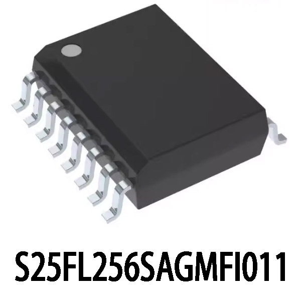
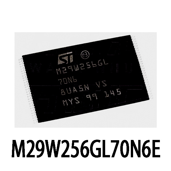
| Parameter | XCF32PVOG48C | XCF16PVOG48C | S25FL256SAGMFI011 | M29W256GL70N6E |
|---|---|---|---|---|
| Vendor | Xilinx | Xilinx | Cypress / Infineon | Micron |
| Type | Platform Flash PROM | Platform Flash PROM | SPI NOR Flash | Parallel NOR Flash |
| Capacity | 32 Mbit (4MB) | 16 Mbit (2MB) | 256 Mbit (32MB) | 256 Mbit (32MB) |
| Interface | Serial / Parallel + JTAG | Serial / Parallel + JTAG | SPI (x1/x2/x4) | 16-bit Parallel NOR |
| Operating Voltage | 2.5V | 2.5V | 3.0V | 1.8V / 3.0V |
| FPGA Support | Spartan / Virtex | Spartan / Virtex | Supports Spartan-6/7 via SPI | Supports Virtex via BPI |
| Package | VQFP-48 | VQFP-48 | SOIC-16 / BGA | TSOP56 / VFBGA |
| JTAG Support | ✅ Yes | ✅ Yes | ❌ Requires programmer or host write | ❌ |
| Multiboot Support | ✅ Supported | ✅ Supported | ✅ Supported (via SPI) | ✅ Supported |
| Recommended Use | Traditional Xilinx configuration PROM | Low-capacity PROM replacement | SPI boot for Artix-7 and similar | High-speed parallel configuration |
If you’re using XCF32PVOG48C but need a replacement, here’s what I’d suggest: For older Spartan-3/6 designs with fixed space, just use XCF16PVOG48C—same package, half the capacity. For new projects like Artix-7 or Zynq, switch to larger and cheaper SPI Flash such as S25FL series, but note you can’t program these directly via JTAG. For high-end Virtex requiring BPI mode, M29W256GL works, though it’s bigger and more complicated.
XCF32PVOG48C JTAG Programming Circuit

Check out this schematic—it’s a typical JTAG programming circuit for the XCF32PVOG48C chip, perfect for configuring your FPGA. The JTAG pins (TDI, TMS, TCK, TDO) go straight to your programmer, making it easy with Vivado or iMPACT. Keep your power lines separate: 3.3V for VCCO and JTAG (VCCJ), 1.8V for VCCINT, and don’t forget decoupling capacitors nearby for stable operation. Also, use a 10kΩ resistor (and optionally a capacitor) to pull the RESET pin high to avoid unintended resets. This design is straightforward and reliable.
XCF32PVOG48C SPI Boot Configuration
If you’re planning SPI boot for Artix-7, Spartan-7, or Zynq FPGA, the XCF32PVOG48C won’t work. It’s only compatible with older modes like Master Serial, Slave Serial, or SelectMAP, but lacks SPI support. Instead, choose dedicated SPI Flash chips like S25FL256S, MT25QL128, or W25Q128—these chips perfectly fit SPI boot applications and are both affordable and widely compatible.
XCF32PVOG48C FPGA Board Wiring
If you want your FPGA to automatically load configurations at startup, XCF32PVOG48C Platform Flash PROM is your go-to solution. Connect DQ0 to FPGA’s DIN, CCLK to FPGA’s CCLK, and pull CS low. OE/RESET pin should be pulled high or connected to FPGA INIT_B. Programming is easy through JTAG using Vivado or iMPACT. For power, supply 1.8V for the core and 3.3V for IO and JTAG. Remember to place 0.1μF and 4.7μF decoupling capacitors close to the power pins to keep signals clean.
XCF32PVOG48C Multiple FPGA Programming
If you’re configuring multiple FPGAs from a single XCF32PVOG48C PROM, try using a daisy-chain setup. For instance, connect PROM’s DQ0 to the first FPGA’s DIN, then link its DOUT to the next FPGA’s DIN, sharing the same CCLK line. All FPGA DONE pins connect together to signal successful configuration. Combine your bitstreams using Vivado or iMPACT before programming the PROM. Keep clock and signal lines short to reduce interference and ensure stable operation.
More Like This

MC5430F
Motorola

JD54LS51BCA
National Semiconductor

USPLSI2032VE-110LB49
Lattice Semiconductor Corporation
74S22PC
Rochester Electronics, LLC

9504DC
National Semiconductor

9005PC
National Semiconductor

9007DC
National Semiconductor
9004DC
National Semiconductor

SN74HC804DWR
Texas Instruments
SN700863DWR
Texas Instruments
4001BDMQB
National Semiconductor
54F02FMQB
National Semiconductor
Also Add to Cart

74LCX245MTR
STMicroelectronics

XC9141B26CMR-G
Torex Semiconductor Ltd

LP87332DRHDT
Texas Instruments

MAX7312AUG+T
Analog Devices Inc./Maxim Integrated
74ABT2244CSCX
onsemi

MAX818MESA+
Analog Devices Inc./Maxim Integrated

LC4064C-10TN100I
Lattice Semiconductor Corporation

TPS65133DPDR
Texas Instruments

ADP5034AREZ-1
Analog Devices Inc.

SN74ACT7201LA50RJ
Texas Instruments

MIC2580A-1.6BTS-TR
Microchip Technology

74VHC32MTCX
onsemi
Related Products
MC5430F
Motorola
JD54LS51BCA
National Semiconductor
USPLSI2032VE-110LB49
Lattice Semiconductor Corporation
74S22PC
Rochester Electronics, LLC
9504DC
National Semiconductor
9005PC
National Semiconductor
9007DC
National Semiconductor
9004DC
National Semiconductor
SN74HC804DWR
Texas Instruments
SN700863DWR
Texas Instruments
4001BDMQB
National Semiconductor
54F02FMQB
National Semiconductor
DM54S20W/883
National Semiconductor

MC3129L
Motorola
4071BDM
National Semiconductor
MC9814P
Motorola
MC9825P
Motorola

74AC11000NS
Texas Instruments
MC5420L
Motorola
MC5401L
Motorola
MC5401F
Motorola
SN74H61N
Texas Instruments
MC5410F
Motorola
MC5430L
Motorola

SN74AS138N-J
Texas Instruments
CD4023BCN
Fairchild Semiconductor
4019BDC
National Semiconductor
74H40DC
National Semiconductor
5420FMQB
National Semiconductor
4025BDM
National Semiconductor
Please send RFQ , we will respond immediately.
