
BD140 datasheet | pinout, equivalent & transistor circuit | price & pdf STMicroelectronics
- Transistor Type: PNP
- Current-Collector(Ic)(Max): 1.5 A
- Voltage-Collector Emitter Breakdown (Max): 80 V
- Package: TO-225AA, TO-126-3


FREE delivery for orders over HK$250.00

Quick response, quick quotaton

Flash shipment,no worries after sales

Original channel,guarantee of the authentic products
BD140
BD140 Pinout
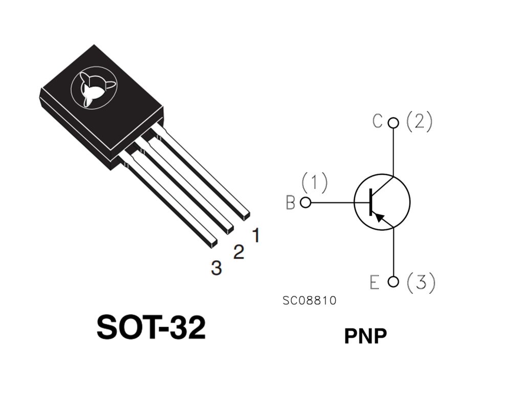
BD140 Pinout Diagram
The BD140 is a PNP transistor commonly used for amplification and switching applications. It features three main terminals: the Base (B), Collector (C), and Emitter (E). The pinout configuration is designed to control the flow of current and manage the transistor’s switching behavior in various electronic circuits.
| Pin Number | Pin Name | Description |
|---|---|---|
| 1 | Base (B) | The base terminal controls the current flow between the collector and emitter. It is used to turn the transistor on or off. |
| 2 | Collector (C) | The collector terminal is where the majority of the current flows through the transistor. It’s connected to the load. |
| 3 | Emitter (E) | The emitter terminal is the output for the current and is connected to the negative side of the circuit. |
In conclusion, the BD140’s pinout configuration is fundamental to its proper functioning in a circuit. The base, collector, and emitter work together to control the current flow, making the transistor ideal for use in power control and amplification tasks.
More Like This

JANTXV2N5238S
Microchip Technology

JANTXV2N5238
Microchip Technology
JANTXV2N5237S
Microchip Technology
JAN2N2906AUA
Microchip Technology
2N918UB
Microchip Technology

JANKCA2N2369A
Microchip Technology
2N1711S
Microchip Technology

JANKCB2N3440
Microchip Technology
JANKCB2N3439
Microchip Technology
JAN2N918UB/TR
Microchip Technology
JANTXV2N5154P
Microchip Technology
JANTXV2N5153P
Microchip Technology
Also Add to Cart

BD681STU-ON
onsemi

FZT749QTA
Diodes Incorporated

MJD210G
onsemi
.JPG "BD138")
BD138
STMicroelectronics
2N5238
Microchip Technology

JAN2N3501UB
Microchip Technology

FCX2016TC
Diodes Incorporated

NTE2350
NTE Electronics, Inc

KST43MTF
Fairchild Semiconductor

2SB815-6-TB-E
onsemi

KSA1013OTA
Fairchild Semiconductor

2SA1588-Y,LF
Toshiba Semiconductor and Storage
Related Products
JANTXV2N5238S
Microchip Technology
JANTXV2N5238
Microchip Technology
JANTXV2N5237S
Microchip Technology
JAN2N2906AUA
Microchip Technology
2N918UB
Microchip Technology
JANKCA2N2369A
Microchip Technology
2N1711S
Microchip Technology
JANKCB2N3440
Microchip Technology
JANKCB2N3439
Microchip Technology
JAN2N918UB/TR
Microchip Technology
JANTXV2N5154P
Microchip Technology
JANTXV2N5153P
Microchip Technology
JAN2N918UB
Microchip Technology
JANTX2N3634UB/TR
Microchip Technology
JANTX2N2369AUB/TR
Microchip Technology
JANTX2N2222AUA/TR
Microchip Technology
JANTX2N3634UB
Microchip Technology

JANTX2N2369AUB
Microchip Technology
2N3501L
Microchip Technology

JANTX2N2605
Microchip Technology
JAN2N3439P
Microchip Technology
JANTX2N2222AUA
Microchip Technology

2N5680L
Microchip Technology

2N5680
Microchip Technology
2N5415
Microchip Technology
2N2946
Microchip Technology
2N2945A
Microchip Technology
JANTXV2N3439P
Microchip Technology

JANTXV2N2484UA/TR
Microchip Technology
2N3725UB/TR
Microchip Technology
Please send RFQ , we will respond immediately.
