
XCF32PFSG48C fiche technique et pdf | prix
- Marques : AMD Xilinx
- Télécharger: -
- Prix: enquête
- En stock: 7440
- Statut du produit : Obsolète
- Type programmable : Dans le système programmable
- Taille de la mémoire : 32Mb
- Emballer: 48-TFBGA, CSPBGA


Livraison GRATUITE pour les commandes supérieures à HK$250.00

Réponse rapide, devis rapide

Expédition rapide, pas de soucis après-vente

Chaîne originale, garantie de produits authentiques
XCF32PFSG48C
The XCF32PFSG48C is a low-power, high-speed CPLD from Xilinx’s CoolRunner-II family. It’s designed for efficient performance in battery-powered or energy-sensitive applications. With 32 macrocells, it handles both combinatorial and sequential logic tasks. This device operates at 3.3V, supports 2.5V logic levels, and is packaged in a 48-pin Fine-Pitch Ball Grid Array (FBGA), making it compatible with many systems.
It’s capable of speeds up to 200 MHz, ideal for digital signal processing or control. You can easily configure it using the JTAG interface, and the best part is that it’s in-system programmable, meaning you don’t need to remove it from your circuit to update its configuration. Whether for signal processing, state machine design, or interface bridging, the XCF32PFSG48C offers flexibility and efficiency.
XCF32PFSG48C Equivalent FPGA Config Flash
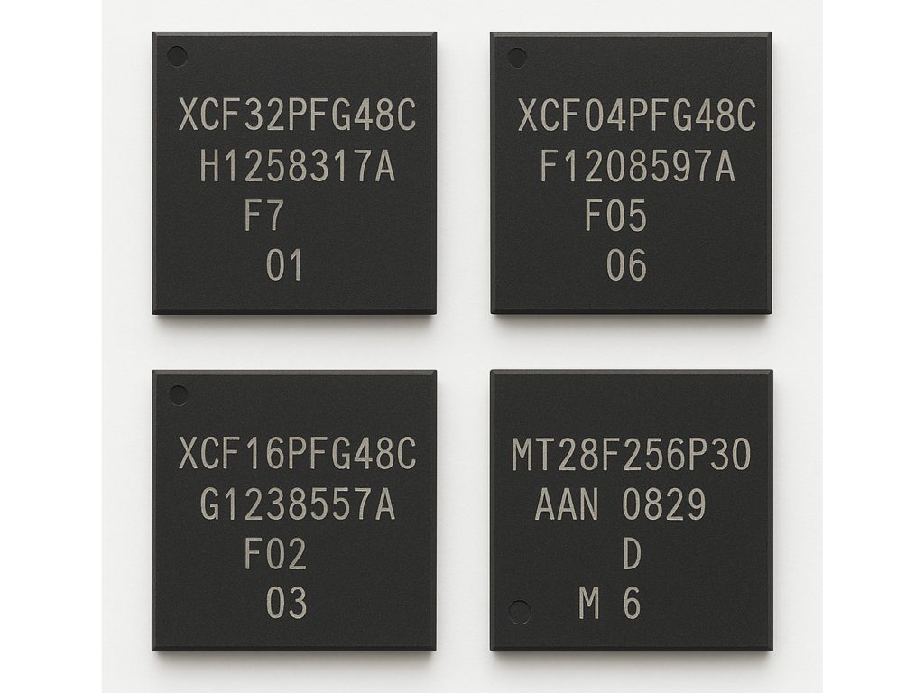
| Paramètre | XCF32PFSG48C | XCF04PFG48C | XCF16PFG48C | MT28F256P30 |
|---|---|---|---|---|
| Type de colis | 48-pin FBGA | 48-pin FBGA | 48-pin FBGA | 48-pin TSOP |
| Memory Size | 32Mb | 4 Mo | 16 Mo | 32Mb |
| Voltage Range | 2.5V to 3.6V | 2.5V to 3.6V | 2.5V to 3.6V | 3.0V to 3.6V |
| Interface | SPI, JTAG | SPI, JTAG | SPI, JTAG | SPI, Parallel |
| Data Bus Width | 1-bit | 1-bit | 1-bit | 8-bit |
| Vitesse | 66 MHz | 66 MHz | 66 MHz | 60 MHz |
| Temperature Range | Commercial (0°C to 70°C) | Commercial (0°C to 70°C) | Commercial (0°C to 70°C) | Industrial (-40°C to 85°C) |
| Features | In-System Programmable, Low Power | In-System Programmable, Low Power | In-System Programmable, Low Power | In-System Programmable, High-Density |
If you’re looking for alternatives to the XCF32PFSG48C, the XCF04PFG48C and XCF16PFG48C are great choices for lower memory applications. They still offer similar functionality—like SPI, JTAG, and low power—so if your design only needs 4Mb or 16Mb of memory, these might be perfect. But keep in mind, they can’t handle designs as large as the XCF32PFSG48C.
On the other hand, the MT28F256P30 offers a parallel data bus, which can boost data throughput for certain applications. But it does come with a slightly higher voltage range and lower SPI speed, which could impact performance depending on your needs.
XCF32PFSG48C FPGA Programming Circuit

In this diagram, here’s how the key components and connections work:
-
VCC (3.3V): Powers the FPGA, providing the necessary voltage.
-
4.7μF Capacitor: Helps smooth out any power noise, ensuring stable operation.
-
TDI, TMS, TCK, TDO, RESET Pins: These are part of the JTAG interface, used for programming and debugging the FPGA. Data flows through the TDI, TMS, and TCK pins, while the TDO pin sends data back.
-
CE and CF Pins (Chip Enable and Configuration Flash): Control whether the FPGA is being configured.
-
VCCINT, VCCO: These power pins supply different voltages for internal logic (VCCINT) and I/O buffers (VCCO).
-
GND: Ground connections to complete the circuit.
This setup is typical for JTAG-based programming. The reset pin ensures everything starts correctly, while the capacitor keeps the voltage stable during configuration.
XCF32PFSG48C Board Layout Example
When placing your main components, put the XCF32PFS48C close to your FPGA. Keep the configuration lines (TDI, TMS, TCK, TDO) short and straight to avoid interference or delays.
For the power setup, connect VCCJ and VCCO to 3.3V with 0.1μF and 4.7μF decoupling capacitors close to the pins. Connect VCCINT to a stable 1.8V supply, ideally isolated to prevent voltage instability on your FPGA.
With the JTAG interface, run TDI, TMS, TCK, and TDO directly from a standard 2.54mm pin header to both FPGA and XCF32P. It’s helpful to include a RESET line with a 10kΩ pull-up resistor for easier debugging.
For CE and CF pins, tie them to ground or pull them up depending on your external Flash configuration needs. If cascading multiple devices, pull CF high so the main device recognizes this one.
Lastly, make sure all ground pins are connected solidly to the ground plane. Add bypass capacitors near all power pins. Keep routing clean, avoid flying wires, and minimize 90-degree turns on JTAG lines.
XCF32PFSG48C Boot-Up Memory Setup
Here’s how to set up the boot-up memory for the XCF32PFS48C FPGA:
-
Power-Up: Make sure both the FPGA and XCF32PFS48C get the right power. The FPGA needs 3.3V (VCCO) and the XCF32PFS48C needs 1.8V (VCCINT). Don’t forget decoupling capacitors (0.1µF and 4.7µF) near the power pins for stable power.
-
Configuration Mode: Pull the CE pin low to enable the device. For CF, connect it to ground or VCC based on your setup.
-
JTAG Interface (Optional): If using JTAG for programming, ensure TDI, TMS, TCK, TDO are connected properly.
-
Memory Initialization: Once powered up, the FPGA reads the configuration from the XCF32PFS48C and loads it.
-
Programming: If the XCF32PFS48C isn’t pre-programmed, use JTAG to load the configuration.
-
Status Monitoring: Utiliser BUSY et DONE pins to check the boot process. When DONE goes high, configuration is complete.
Plus comme ça

ZXCW6100S28
Diodes Incorporées

TDA8541T/N1,112
NXP USA Inc.

TDA8541T/N1,118
NXP USA Inc.

TDA7056B/N1,112
NXP USA Inc.
,SOT157-2.JPG "TDA2616Q/N1,112")
TDA2616Q/N1,112
NXP USA Inc.

TDA8547TS/N1,112
NXP USA Inc.
TDA8547TS/N1,118
NXP USA Inc.

NE58633BS,157
NXP USA Inc.
NE58633BS,115
NXP USA Inc.

SA58670BS,115
NXP USA Inc.

TS4961TIQT
STMicroelectronics
,SOT523-1.JPG "TFA9842J/N1,112")
TFA9842J/N1,112
NXP USA Inc.
Ajouter également au panier

1SX165HN3F43E2VG
Intel

SI3404-A-GM
Skyworks Solutions Inc.

IR21592PBF
Infineon Technologies

HMC910LC4BTR-R5
Analog Devices Inc.

EN80C188XL-20
Rochester Electronics, LLC

LTC4311ISC6#TRMPBF
Analog Devices Inc.

BD7836EFV-E2
Semi-conducteurs Rohm

ISL95837HRZ
Renesas Electronics America Inc

PEF41068FV1.1
Lantiq
MPC8377VRAJFA
NXP USA Inc.

CP2114-B01-GM
Laboratoires de silicium

OPA330AIYFFR
Texas Instruments
Produits connexes
ZXCW6100S28
Diodes Incorporées
TDA8541T/N1,112
NXP USA Inc.
TDA8541T/N1,118
NXP USA Inc.
TDA7056B/N1,112
NXP USA Inc.
TDA2616Q/N1,112
NXP USA Inc.
TDA8547TS/N1,112
NXP USA Inc.
TDA8547TS/N1,118
NXP USA Inc.
NE58633BS,157
NXP USA Inc.
NE58633BS,115
NXP USA Inc.
SA58670BS,115
NXP USA Inc.
TS4961TIQT
STMicroelectronics
TFA9842J/N1,112
NXP USA Inc.

SA58632BS,118
NXP USA Inc.

TDA1308TT/N2,118
NXP USA Inc.
TDA8552TS/N1,112
NXP USA Inc.
TDA8552TS/N1,118
NXP USA Inc.
TDA1517/N3,112
NXP USA Inc.
TDA7056A/N2,112
NXP USA Inc.

SA58671UK,027
NXP USA Inc.

TDA8948J/N1,112
NXP USA Inc.
TFA9843AJ/N1,112
NXP USA Inc.

SA58637BS,118
NXP USA Inc.

TDA7052A/N2,112
NXP USA Inc.

TDA8551T/N1,112
NXP USA Inc.

TDA8551T/N1,118
NXP USA Inc.
SA58672UK,027
NXP USA Inc.
SA58670ABS,115
NXP USA Inc.

SA58631TK,157
NXP USA Inc.
SA58631TK,118
NXP USA Inc.
SA58631TK,115
NXP USA Inc.
Veuillez envoyer une demande de devis, nous vous répondrons immédiatement.
