
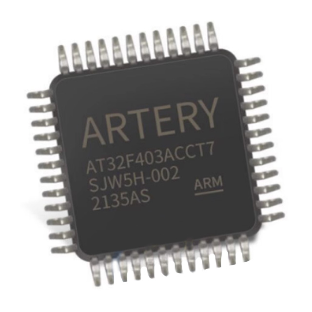
AT32F403ACCT7 datasheet, price & review
- I/O की संख्या: -
- सीपीयू अधिकतम गति: -
- डीएसी (बिट): -
- पैकेट: LQFP-48(7x7)


HK$250.00 से अधिक ऑर्डर पर निःशुल्क डिलीवरी

त्वरित प्रतिक्रिया, त्वरित उद्धरण

फ्लैश शिपमेंट, बिक्री के बाद कोई चिंता नहीं

मूल चैनल, प्रामाणिक उत्पादों की गारंटी
Reprogram at32f403 hoverboard with st-link
At32f403acct7
If you’re looking into a versatile and powerful microcontroller for your next project, the AT32F403ACCT7 from Artery might be just what you need. Built around the ARM Cortex-M4 core, it runs at speeds up to 240 MHz and includes a built-in hardware floating-point unit (FPU), making it ideal for real-time processing tasks.
With 256KB of flash memory and 96KB SRAM, you’ve got plenty of room for your code and data. It offers a broad operating voltage range from 2.6V to 3.6V, plus several low-power modes perfect for battery-powered applications.
You’ll appreciate its extensive peripheral set, including multiple timers, USART, UART, SPI, I²C, USB 2.0 (with OTG support), and CAN interfaces—perfect for industrial communications. Its high-speed 12-bit ADC (up to 2.6Msps) and 12-bit DAC are excellent for precision measurement and control applications.
Just remember: ensure clean power supply lines for stable operation, isolate your analog circuits for accuracy, and handle USB interface signals carefully. The AT32F403ACCT7 is a solid choice for industrial automation, IoT devices, and intelligent electronics, offering great performance at an affordable price.
At32f403acct7 Pinout

| Pin No. | पिन नाम | विवरण |
|---|---|---|
| 1 | VSSA | Analog Ground |
| 2 | VDDA | Analog Power Supply |
| 3 | PA0 | GPIO, supports ADC_IN0, USART2_CTS, TMR2_CH1, etc. |
| 4 | PA1 | GPIO, supports ADC_IN1, USART2_RTS, TMR2_CH2, etc. |
| 5 | PA2 | GPIO, supports ADC_IN2, USART2_TX, TMR2_CH3, etc. |
| 6 | PA3 | GPIO, supports ADC_IN3, USART2_RX, TMR2_CH4, etc. |
| 7 | PA4 | GPIO, supports ADC_IN4, SPI1_NSS, DAC_OUT1, etc. |
| 8 | PA5 | GPIO, supports ADC_IN5, SPI1_SCK, TMR2_CH1_ETR, etc. |
| 9 | PA6 | GPIO, supports ADC_IN6, SPI1_MISO, TMR3_CH1, etc. |
| 10 | PA7 | GPIO, supports ADC_IN7, SPI1_MOSI, TMR3_CH2, etc. |
| 11 | PB0 | GPIO, supports ADC_IN8, TMR3_CH3, DAC_OUT1, etc. |
| 12 | PB1 | GPIO, supports ADC_IN9, TMR3_CH4, DAC_OUT2, etc. |
| 13 | PB2 | GPIO, supports BOOT1, TMR2_CH3, etc. |
| 14 | PB10 | GPIO, supports I2C2_SCL, USART3_TX, TMR2_CH3, etc. |
| 15 | PB11 | GPIO, supports I2C2_SDA, USART3_RX, TMR2_CH4, etc. |
| 16 | VSS | Digital Ground |
| 17 | वीडीडी | Digital Power Supply |
| 18 | PA8 | GPIO, supports USART1_CK, TMR1_CH1, etc. |
| 19 | PA9 | GPIO, supports USART1_TX, TMR1_CH2, etc. |
| 20 | PA10 | GPIO, supports USART1_RX, TMR1_CH3, etc. |
| 21 | PA11 | GPIO, supports USART1_CTS, CAN_RX, TMR1_CH4, etc. |
| 22 | PA12 | GPIO, supports USART1_RTS, CAN_TX, TMR1_ETR, etc. |
| 23 | PA13 | GPIO, JTAG/SWD Interface: JTMS/SWDIO |
| 24 | PA14 | GPIO, JTAG/SWD Interface: JTCK/SWCLK |
| 25 | PA15 | GPIO, JTAG Interface: JTDI |
| 26 | PB3 | GPIO, JTAG Interface: JTDO, TMR2_CH2, etc. |
| 27 | PB4 | GPIO, JTAG Interface: NJTRST, TMR3_CH1, etc. |
| 28 | PB5 | GPIO, supports I2C1_SMBA, TMR3_CH2, etc. |
| 29 | PB6 | GPIO, supports I2C1_SCL, USART1_TX, TMR4_CH1, etc. |
| 30 | PB7 | GPIO, supports I2C1_SDA, USART1_RX, TMR4_CH2, etc. |
| 31 | PB8 | GPIO, supports TMR4_CH3, CAN_RX, etc. |
| 32 | PB9 | GPIO, supports TMR4_CH4, CAN_TX, etc. |
| 33 | VSS | Digital Ground |
| 34 | वीडीडी | Digital Power Supply |
| 35 | PC13 | GPIO, supports RTC_AF1, etc. |
| 36 | PC14 | GPIO, supports OSC32_IN (Low-Speed External Crystal Input) |
| 37 | PC15 | GPIO, supports OSC32_OUT (Low-Speed External Crystal Output) |
| 38 | PD0 | GPIO, supports OSC_IN (High-Speed External Crystal Input) |
| 39 | PD1 | GPIO, supports OSC_OUT (High-Speed External Crystal Output) |
| 40 | NRST | Reset Pin |
When you’re working with the AT32F403ACCT7 microcontroller, remember each pin often serves multiple functions like GPIO, ADC, USART, or SPI. So, choose the right function based on your design to avoid conflicts. Make sure you properly connect all power and ground pins (like VDD, VDDA, VSS, and VSSA). Place decoupling capacitors near these pins—it really helps keep things stable.
Also, pay special attention to the NRST pin; adding a pull-up resistor and capacitor gives you a solid, reliable startup every time you power up the board. For debugging, PA13 and PA14 are your SWD pins. If you’re not debugging, you can reuse these as GPIOs, but be cautious that you don’t mess up other functionalities.
Unused pins shouldn’t be left floating—set them as inputs with pull-ups or pull-downs, or outputs driven low. Lastly, most GPIO pins can handle 5V, but always double-check the voltage levels to avoid accidentally damaging your chip.
At32f403acct7 Equivalent Cortex Mcu
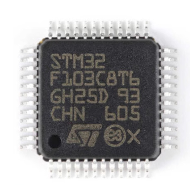
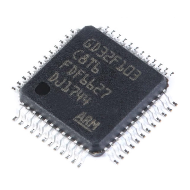
| पैरामीटर | AT32F403ACCT7 | STM32F103C8T6 | GD32F103C8T6 |
|---|---|---|---|
| Core | Cortex-M4 (with FPU) | Cortex-M3 | Cortex-M3 |
| Clock Speed | 240 MHz | 72 MHz | 108 MHz |
| Flash Size | 256 KB | 64/128 KB | 64 KB |
| SRAM Size | 224 KB (96+128 KB) | 20 KB | 20 KB |
| GPIO Pins | 37 | 37 | 37 |
| ADC Channels | 3 ADCs, max 16 channels | 2 ADCs, max 10 channels | 2 ADCs, max 10 channels |
| Timers | 17 timers | 7 timers | 7 timers |
| Communication Interfaces | USART, SPI, I2C, CAN, USB | USART, SPI, I2C, CAN, USB | USART, SPI, I2C, CAN, USB |
| पैकेज का प्रकार | LQFP-48 (7×7 mm) | LQFP-48 (7×7 mm) | LQFP-48 (7×7 mm) |
| Operating Voltage | 2.6V ~ 3.6V | 2.0V ~ 3.6V | 2.0V ~ 3.6V |
| Temperature Range | -40°C ~ 105°C | -40° सेल्सियस ~ 85° सेल्सियस | -40° सेल्सियस ~ 85° सेल्सियस |
| Floating Point Support | Yes (with FPU) | नहीं | नहीं |
| Clock Priority | Best | Inferior | Moderate |
| अनुकूलता | Compatible with STM32F103 | Compatible with GD32F103 | Compatible with STM32F103 |
When swapping out chips like the STM32F103C8T6, you’ll find that the AT32F403ACCT7 and GD32F103C8T6 fit right in, especially since they all come in the same LQFP-48 package. The AT32F403ACCT7 really shines if you need more power, with a faster clock speed (240 MHz) and a larger SRAM (224 KB), which makes it perfect for high-performance applications. The GD32F103C8T6 runs at 108 MHz, offering a nice step up from the STM32F103C8T6’s 72 MHz. When it comes to software, GD32F103C8T6 is highly compatible with STM32 tools, but for the AT32F403ACCT7, you’ll need tools from Artery. Also, keep in mind that the AT32F403ACCT7 supports a wider temperature range, making it great for industrial use.
At32f403acct7 Development Board Wiring
Here’s a quick guide to setting up your AT32F403ACCT7. First, connect the power pins—VDD (pin 48) and VDDA (pin 47)—to a 3.3V power supply, and don’t forget the ground pins, VSSA (pin 1) and VSS (pin 16), which should go to the power ground. Place a 100nF decoupling capacitor near the power pins for stability. If you’re using USB power, just connect the USB port for both power and data.
For debugging and programming, use the SWD interface (SWDIO on pin 19 and SWCLK on pin 18) with a tool like ST-Link. The GPIO pins (PA0-PA15, PB0-PB15, PC13-PC15, PD0-PD1) are perfect for connecting external devices like sensors or LEDs.
You can also use communication interfaces like USART for serial, SPI for devices like sensors, or I2C for displays. For reset functionality, connect the NRST pin to 3.3V with a 10kΩ pull-up resistor.
At32f403acct7 Usb Application Example
The AT32F403ACCT7 microcontroller comes with a Full-Speed USB 2.0 device interface, which opens up a lot of possibilities for USB-based applications, like USB HID (Human Interface Devices) and USB Mass Storage.
For example, with USB HID, you can easily turn the AT32F403ACCT7 into a keyboard or mouse. Just connect the USB D+ and D- pins to the host, and using the USB HID protocol, you can simulate key presses or mouse movements.
Another great application is using it as a USB Mass Storage device. You can connect the AT32F403ACCT7 to external storage like an SD card or flash memory, and make it work like a USB flash drive, allowing you to read and write files to the storage.
Just remember to use a USB protocol stack (like STMicroelectronics’ library), ensure the USB host is providing stable 5V power, and properly connect the VBUS pin. With these simple setups, you can create powerful USB peripherals with ease.
At32f403acct7 Timer and Pwm Usage
The AT32F403ACCT7 microcontroller has several timer modules, including advanced and general-purpose timers, which make it great for precise timing, counting, and generating PWM signals. These timers are super useful in embedded systems for things like periodic tasks, signal generation, and device control.
For example, the timers can trigger interrupts at set intervals, capture timestamps from external signals, or generate output compares. You can use them to create regular interrupts for timed tasks.
When it comes to PWM, the timers’ output compare function lets you generate PWM signals. This is commonly used for controlling motors or dimming LEDs. You can easily adjust the PWM frequency and duty cycle by configuring the timers, giving you full control over the signal.
With flexible timer settings, including pre-scaling and counters, the AT32F403ACCT7 allows for precise control to meet a wide range of needs in your projects.
At32f403acct7 I2c and Spi Connection
Let’s break down the I2C and SPI interfaces on the AT32F403ACCT7 and when you might use each.
At32f403acct7 Boot Setup
When working with the AT32F403ACCT7, you’ll want to set up the boot mode, which determines where the microcontroller loads its startup program from. This is done through the BOOT0 and BOOT1 pins.
-
BOOT0 Pin: If you set BOOT0 to 0, the microcontroller will boot from internal flash (the default). If you set it to 1, it’ll look for an external device, like SPI flash or a serial bootloader.
-
BOOT1 Pin: This pin is used for more complex startup options. With BOOT1 set to 0, it defaults to booting from internal flash. If set to 1, it tries to boot from other external devices (like a serial interface).
Based on the combination of these two pins, the microcontroller will select its boot mode:
-
0, 0: Boots from internal flash.
-
0, 1: Boots from system memory (used for bootloaders).
-
1, 0: Boots from external devices like SPI flash.
-
1, 1: Reserved for special cases.
For firmware updates or loading applications from external storage, you can modify these pins to choose your preferred boot source.
At32f403acct7 Keil Code Example
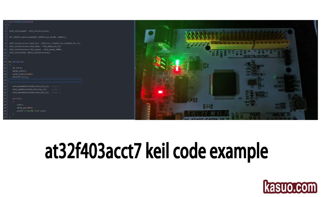
Code Example:
void AT32LED_Init(void)
{
GPIO_InitTypeDef GPIO_InitStructure;
RCC_APB2PeriphClockCmd(RCC_APB2Periph_GPIO, ENABLE);
GPIO_InitStructure.GPIO_Pin = GPIO_Pin_13 | GPIO_Pin_14 | GPIO_Pin_15;
GPIO_InitStructure.GPIO_Mode = GPIO_Mode_Out_PP;
GPIO_InitStructure.GPIO_Speed = GPIO_Speed_50MHz;
GPIO_Init(GPIO, &GPIO_InitStructure);
AT91F1_Init();
}
int main(void)
{
u8 cut = 0;
delay_init(168000);
uart_init(115200);
AT91F1_Init();
GPIO_ResetBits(GPIO, GPIO_Pin_13); // LED1 OFF
GPIO_SetBits(GPIO, GPIO_Pin_14); // LED2 ON
GPIO_ResetBits(GPIO, GPIO_Pin_15); // LED3 OFF
while(1)
{
cut++;
delay_ms(1000);
printf(“cut:%d \r\n”, cut);
}
}
This code is written for embedded systems, like the AT32 series microcontroller, to control GPIO pins and light up an LED.
Here’s a Quick Breakdown of How It Works:
Initialization: The AT32LED_Init() function sets up the GPIO pin that controls the LED. It configures the pin as an output, setting the speed to 50 MHz. The RCC_APB2PeriphClockCmd() function enables the clock for the GPIO peripherals, allowing you to use them.
Main Function: The main() function starts by initializing a counter and setting up the delay function and UART for serial communication. Inside a loop, it toggles the LED by using GPIO_ResetBits() (to turn it off) and GPIO_SetBits() (to turn it on), with a 1-second delay between toggles.
GPIO & UART: The GPIO pins are used to control the LED, while UART might be used for debugging or monitoring.
Summary: Essentially, this code sets up the GPIO pins to control the LED, and it uses UART to send out the counter value for monitoring. It’s a simple example of using GPIO and UART together.
At32f403acct7 Low Power Config
The AT32F403ACCT7 microcontroller offers several low-power modes to help you save energy and extend battery life. Here’s a quick rundown:
-
स्लीप मोड: The CPU stops processing, but peripherals like timers and I2C continue to run. This is perfect for applications that only need to perform periodic tasks. To enter sleep mode, set the SLEEPDEEP bit and use the
__WFI()command. -
Stop Mode: In this mode, the CPU and most peripherals are turned off, but critical peripherals like external interrupts remain active. It’s great for situations where you want to stop the CPU but keep a few devices awake. Use the PWR_CR register to configure it.
-
आधार रीति: This is the lowest power mode, where most peripherals are turned off except for things like RTC and external interrupts. Use the PWR_CR register to enter standby.
Additionally, you can disable unnecessary peripherals, reduce clock speeds, and use low-power clock sources to further save power. You can wake the system using external interrupts, timers, or RTC interrupts.
इसी तरह और भी

ZXCW6100S28
डायोड्स इन्कॉर्पोरेटेड

TDA8541T/N1,112
एनएक्सपी यूएसए इंक.

TDA8541T/N1,118
एनएक्सपी यूएसए इंक.

TDA7056B/N1,112
एनएक्सपी यूएसए इंक.
,SOT157-2.JPG "TDA2616Q/N1,112")
TDA2616Q/N1,112
एनएक्सपी यूएसए इंक.

TDA8547TS/N1,112
एनएक्सपी यूएसए इंक.
TDA8547TS/N1,118
एनएक्सपी यूएसए इंक.

NE58633BS,157
एनएक्सपी यूएसए इंक.
NE58633BS,115
एनएक्सपी यूएसए इंक.

SA58670BS,115
एनएक्सपी यूएसए इंक.

TS4961TIQT
एसटीमाइक्रोइलेक्ट्रॉनिक्स
,SOT523-1.JPG "TFA9842J/N1,112")
TFA9842J/N1,112
एनएक्सपी यूएसए इंक.
कार्ट में भी जोड़ें

EPM7064AETI100-7AA
इंटेल

AD8639ARZ-REEL7
एनालॉग डिवाइसेज इंक.

SC16C754IB80,551
एनएक्सपी यूएसए इंक.
XC95216-20PQ160I
एएमडी ज़िलिनक्स

MPC8321ECZQADDC
एनएक्सपी यूएसए इंक.
EP610DM-30
रोचेस्टर इलेक्ट्रॉनिक्स, एलएलसी

MC68EC040FE33A
एनएक्सपी यूएसए इंक.
GS1531-CBE2
सेमटेक कॉर्पोरेशन

ADCMP602BRMZ
एनालॉग डिवाइसेज इंक.
M5LV-512/160-6YC
लैटिस सेमीकंडक्टर कॉर्पोरेशन
CYP15G0401RB-BGXC
साइप्रस सेमीकंडक्टर कॉर्प

NCP1399APDR2G
Onsemi
संबंधित उत्पाद
ZXCW6100S28
डायोड्स इन्कॉर्पोरेटेड
TDA8541T/N1,112
एनएक्सपी यूएसए इंक.
TDA8541T/N1,118
एनएक्सपी यूएसए इंक.
TDA7056B/N1,112
एनएक्सपी यूएसए इंक.
TDA2616Q/N1,112
एनएक्सपी यूएसए इंक.
TDA8547TS/N1,112
एनएक्सपी यूएसए इंक.
TDA8547TS/N1,118
एनएक्सपी यूएसए इंक.
NE58633BS,157
एनएक्सपी यूएसए इंक.
NE58633BS,115
एनएक्सपी यूएसए इंक.
SA58670BS,115
एनएक्सपी यूएसए इंक.
TS4961TIQT
एसटीमाइक्रोइलेक्ट्रॉनिक्स
TFA9842J/N1,112
एनएक्सपी यूएसए इंक.

SA58632BS,118
एनएक्सपी यूएसए इंक.

TDA1308TT/N2,118
एनएक्सपी यूएसए इंक.
TDA8552TS/N1,112
एनएक्सपी यूएसए इंक.
TDA8552TS/N1,118
एनएक्सपी यूएसए इंक.
TDA1517/N3,112
एनएक्सपी यूएसए इंक.
TDA7056A/N2,112
एनएक्सपी यूएसए इंक.

SA58671UK,027
एनएक्सपी यूएसए इंक.

TDA8948J/N1,112
एनएक्सपी यूएसए इंक.
TFA9843AJ/N1,112
एनएक्सपी यूएसए इंक.

SA58637BS,118
एनएक्सपी यूएसए इंक.

TDA7052A/N2,112
एनएक्सपी यूएसए इंक.

TDA8551T/N1,112
एनएक्सपी यूएसए इंक.

TDA8551T/N1,118
एनएक्सपी यूएसए इंक.
SA58672UK,027
एनएक्सपी यूएसए इंक.
SA58670ABS,115
एनएक्सपी यूएसए इंक.

SA58631TK,157
एनएक्सपी यूएसए इंक.
SA58631TK,118
एनएक्सपी यूएसए इंक.
SA58631TK,115
एनएक्सपी यूएसए इंक.
कृपया आरएफक्यू भेजें, हम तुरंत जवाब देंगे।
