
SN74LVC1G07DCKR datasheet pdf & price
- Logic Type: Buffer, Non-Inverting
- Number of Elements: 1
- Number of Bit sperElement: 1
- Package: 5-TSSOP, SC-70-5, SOT-353


FREE delivery for orders over HK$250.00

Quick response, quick quotaton

Flash shipment,no worries after sales

Original channel,guarantee of the authentic products
SN74LVC1G07DCKR
The SN74LVC1G07DCKR is a single-channel buffer with an open-drain output. It’s perfect for low-power, high-speed applications. It runs on a supply voltage between 1.65V and 5.5V, so it’s flexible enough for different systems. The open-drain output makes it great for wired-AND logic, which is ideal for bus systems or connecting multiple devices. With a typical delay of just 5ns at 5V, it’s pretty fast. Plus, it sinks up to 32mA, which works for most common applications. It’s also energy-efficient, making it suitable for battery-powered systems. Whether you’re using TTL or CMOS logic, it’s a good fit. Operating in temperatures from -40°C to +125°C means it’s solid even in tough conditions. It’s widely used for tasks like signal isolation, level shifting, and working with open-drain buses like I2C.
SN74LVC1G07DCKR Pinout Map
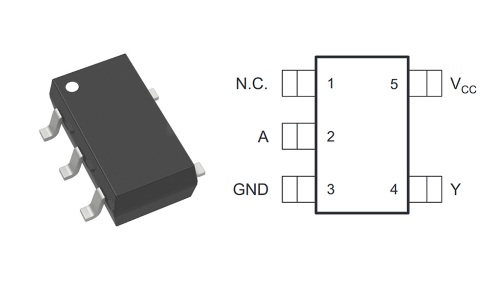
| Pin Number | Pin Name | Description |
|---|---|---|
| 1 | A | Input |
| 2 | GND | Ground |
| 3 | Y | Output (Open-Drain) |
| 4 | NC | No Connection |
| 5 | VCC | Supply Voltage |
Notes:
-
Pin 1 (A): This is the input where you apply the logic signal. It can be HIGH or LOW, and the chip will buffer it to produce an output at Pin 3.
-
Pin 2 (GND): Connect this to ground to complete the circuit.
-
Pin 3 (O): The output, which is open-drain. It either sinks current (goes low) or stays floating (high impedance). If you’re connecting it to other logic or communication lines (like I2C), you’ll need a pull-up resistor.
-
Pin 4 (VCC): The power pin, connected to a voltage source between 1.65V and 5.5V.
Since the output is open-drain, don’t forget that pull-up resistor for proper function, especially when connecting to other devices or buses. It works with both CMOS and TTL systems, so it’s pretty versatile for tasks like signal buffering or level shifting.
SN74LVC1G07DCKR Equivalent Buffer IC

| Parameter | SN74LVC1G07DCKR | 74LVC1G07DCKR | SN74LVC1G125DCKR | 74LVC1G04DCKR |
|---|---|---|---|---|
| Package | DCKR (SOT-23-5) | DCKR (SOT-23-5) | DCKR (SOT-23-5) | DCKR (SOT-23-5) |
| Logic Function | Open-drain buffer | Open-drain buffer | Bus buffer | Inverter |
| Voltage Range | 1.65V to 5.5V | 1.65V to 5.5V | 1.65V to 5.5V | 1.65V to 5.5V |
| Output Type | Open-drain | Open-drain | Push-pull | Inverted push-pull |
| Output Drive | 32mA sink current | 32mA sink current | 32mA sink current | 6mA source/sink |
| Speed (tPD) | 5ns (at 5V) | 5ns (at 5V) | 5ns (at 5V) | 7ns (at 5V) |
| Temperature Range | -40°C to +125°C | -40°C to +125°C | -40°C to +125°C | -40°C to +125°C |
| Logic Compatibility | TTL, CMOS | TTL, CMOS | TTL, CMOS | TTL, CMOS |
Notes:
The SN74LVC1G07DCKR and 74LVC1G07DCKR are pretty much the same. Both are open-drain buffers with similar voltage ranges, current sinking capabilities, and speed, so you can swap them easily.
Now, the SN74LVC1G125DCKR is also an open-drain buffer, but it has a push-pull output. This is important depending on your needs. If your circuit needs an open-drain configuration, stick with the SN74LVC1G07DCKR. But if you need to drive a stronger output signal, the 74LVC1G125DCKR might be the better choice.
As for the 74LVC1G04DCKR, it’s a logic inverter with a push-pull output. It inverts the signal, which makes it different from a simple buffer. If you need signal inversion, it can work as a replacement, but if you just need buffering, it’s not a direct swap.
SN74LVC1G07DCKR Enableable Buffer Circuit

Here’s a simple way to understand the wired OR circuit you’re seeing, built with two SN74LVC1G07DCKR buffers. These buffers are open-drain types, meaning they only actively pull the line down—they don’t push it high. So, to get a high signal, you add a pull-up resistor externally.
The main idea behind “wired OR” is straightforward: you connect outputs from these two buffers together. If either input from your microcontroller or logic device goes low, the entire output line goes low. The pull-up resistor helps ensure the output stays high when neither buffer is pulling it down.
In practice, this setup gives you a neat logical OR effect: the output line stays high unless at least one input signal drops low.
SN74LVC1G07DCKR Signal Buffering Example
-
Level Shifting (Voltage Compatibility): If you’re connecting a 3.3V logic MCU to a 5V system, the 3.3V output might not be enough for the 5V input. The SN74LVC1G07DCKR acts as a buffer, using a pull-up resistor to shift the signal up to 5V when the MCU sends a high signal. This ensures your 3.3V logic works with the 5V system, keeping things safe and reliable.
-
Driving High-Current Loads: If your MCU needs to control a relay or motor that requires more current, the SN74LVC1G07DCKR can buffer the control signal. It can drive a transistor or MOSFET that switches the high-power load, protecting the MCU from direct high-current switching.
More Like This

MC5430F
Motorola

JD54LS51BCA
National Semiconductor

USPLSI2032VE-110LB49
Lattice Semiconductor Corporation
74S22PC
Rochester Electronics, LLC

9504DC
National Semiconductor

9005PC
National Semiconductor

9007DC
National Semiconductor
9004DC
National Semiconductor

SN74HC804DWR
Texas Instruments
SN700863DWR
Texas Instruments
4001BDMQB
National Semiconductor
54F02FMQB
National Semiconductor
Also Add to Cart

74ALVCH16373TX
onsemi

LM4040AIM3X-2.5/NOPB
Texas Instruments
XC6136N47AMR-G
Torex Semiconductor Ltd

CP3BT26G18AWMX/NOPB
Texas Instruments

SN74AHCT541PWRG3
Texas Instruments

LDS6120NQGI
Renesas Electronics America Inc

MIC39301-18BU
Micrel Inc.

SY58034UMI
Microchip Technology

MAX1645BEEI+TG24
Analog Devices Inc./Maxim Integrated

AD8541ARTZ
UMW

S-80856CNMC-B9HT2G
ABLIC Inc.

8N3SV75KC-0081CDI
Renesas Electronics America Inc
Related Products
MC5430F
Motorola
JD54LS51BCA
National Semiconductor
USPLSI2032VE-110LB49
Lattice Semiconductor Corporation
74S22PC
Rochester Electronics, LLC
9504DC
National Semiconductor
9005PC
National Semiconductor
9007DC
National Semiconductor
9004DC
National Semiconductor
SN74HC804DWR
Texas Instruments
SN700863DWR
Texas Instruments
4001BDMQB
National Semiconductor
54F02FMQB
National Semiconductor
DM54S20W/883
National Semiconductor

MC3129L
Motorola
4071BDM
National Semiconductor
MC9814P
Motorola
MC9825P
Motorola

74AC11000NS
Texas Instruments
MC5420L
Motorola
MC5401L
Motorola
MC5401F
Motorola
SN74H61N
Texas Instruments
MC5410F
Motorola
MC5430L
Motorola

SN74AS138N-J
Texas Instruments
CD4023BCN
Fairchild Semiconductor
4019BDC
National Semiconductor
74H40DC
National Semiconductor
5420FMQB
National Semiconductor
4025BDM
National Semiconductor
Please send RFQ , we will respond immediately.
