
STM32F401CCU6 datasheet, pinout & reference manual
- ब्रांड: एसटीमाइक्रोइलेक्ट्रॉनिक्स
- डाउनलोड करना: STM32F401CCU6 Datasheet PDF
- कीमत: जाँच करना
- स्टॉक में: 11,169
- कोरप्रोसेसर: ARM® कॉर्टेक्स®-M4
- कोर आकार: 32-बिट सिंगल-कोर
- बाह्य उपकरण: ब्राउन-आउट डिटेक्ट/रीसेट, DMA, I²S, POR, PWM, WDT
- पैकेट: 48-UFQFN Exposed Pad


HK$250.00 से अधिक ऑर्डर पर निःशुल्क डिलीवरी

त्वरित प्रतिक्रिया, त्वरित उद्धरण

फ्लैश शिपमेंट, बिक्री के बाद कोई चिंता नहीं

मूल चैनल, प्रामाणिक उत्पादों की गारंटी
STM32 Blue Pill vs Black Pill Microcontroller Boards
STM32F401CCU6
STM32F401CCU6 is a well-balanced ARM Cortex-M4 microcontroller, offering good performance at an affordable cost. It’s perfect for medium-complexity embedded projects like IoT nodes, sensor gateways, or battery-powered systems. You get 256KB Flash and 64KB SRAM, plenty for typical control applications. It packs essential peripherals like USART, I²C, SPI, a 10-channel 12-bit ADC, multiple PWM channels and timers, plus a handy USB 2.0 interface for device-mode operations. Its low-power modes make battery operation easy, and the voltage range (2.0V-3.6V) covers most scenarios. Development is smooth with CubeMX or CubeIDE, thanks to ST’s robust ecosystem.
STM32F401CCU6 Pinout Diagram

| पिन नंबर | पिन नाम | Main Function Description |
|---|---|---|
| 1 | वीडीडी | 3.3V Power Input |
| 2 | VDDA | Analog Power Input (for ADC) |
| 3 | PA0 | ADC0, USART2_CTS |
| 4 | PA1 | ADC1, USART2_RTS |
| 5 | PA2 | ADC2, USART2_TX |
| 6 | PA3 | ADC3, USART2_RX |
| 7 | PA4 | ADC4, SPI1_NSS |
| 8 | PA5 | ADC5, SPI1_SCK |
| 9 | PA6 | ADC6, SPI1_MISO |
| 10 | PA7 | ADC7, SPI1_MOSI |
| 11 | PB0 | ADC8, TIM3_CH3 |
| 12 | PB1 | ADC9, TIM3_CH4 |
| 13 | PB2 | BOOT1 (Pull-up/GND to control) |
| 14 | PB10 | I2C2_SCL, USART3_TX |
| 15 | PB11 | I2C2_SDA, USART3_RX |
| 16 | VSS | मैदान |
| 17 | वीडीडी | 3.3V Power Input |
| 18 | PA8 | MCO, TIM1_CH1 |
| 19 | PA9 | USART1_TX |
| 20 | PA10 | USART1_RX |
| 21 | PA11 | USB_DM |
| 22 | PA12 | USB_DP |
| 23 | PA13 | SWDIO (Debug) |
| 24 | PA14 | SWCLK (Debug) |
| 25 | PA15 | SPI1_NSS, TIM2_CH1 |
| 26 | PB3 | SPI1_SCK, TIM2_CH2 |
| 27 | PB4 | SPI1_MISO |
| 28 | PB5 | SPI1_MOSI |
| 29 | PB6 | I2C1_SCL, TIM4_CH1 |
| 30 | PB7 | I2C1_SDA, TIM4_CH2 |
| 31 | BOOT0 | Boot Mode Select (GND for main Flash) |
| 32 | PB8 | I2C1_SCL, TIM4_CH3 |
| 33 | PB9 | I2C1_SDA, TIM4_CH4 |
| 34 | VSS | मैदान |
| 35 | वीडीडी | 3.3V Power Input |
| 36 | PC13 | RTC or GPIO |
| 37 | PC14 | External Crystal OSC32_IN |
| 38 | PC15 | External Crystal OSC32_OUT |
| 39 | PH0 | External Crystal OSC_IN |
| 40 | PH1 | External Crystal OSC_OUT |
| 41 | NRST | Reset Pin |
| 42 | PC0 | GPIO, ADC10 |
| 43 | PC1 | GPIO, ADC11 |
| 44 | PC2 | GPIO, ADC12 |
| 45 | PC3 | GPIO, ADC13 |
| 46 | PC4 | GPIO, ADC14 |
| 47 | PC5 | GPIO, ADC15 |
| 48 | एनसी | Reserved, Not Connected |
The STM32F401CCU6 pins are highly versatile, letting you use USART, I²C, SPI, ADC, and PWM all within just a few pins. When using it, double-check each pin’s default function via STM32CubeMX or CubeIDE to avoid conflicts. Also, make sure not to disable debugging pins (PA13, PA14) accidentally, as you’ll lose debugging access. For USB, PA11 and PA12 must be connected correctly. As for the BOOT0 pin, using a jumper makes switching between main Flash and Bootloader mode easier. If needed, I can also help you convert your table into HTML format for easier uploading.
STM32F401CCU6 Equivalent STM32 Chip

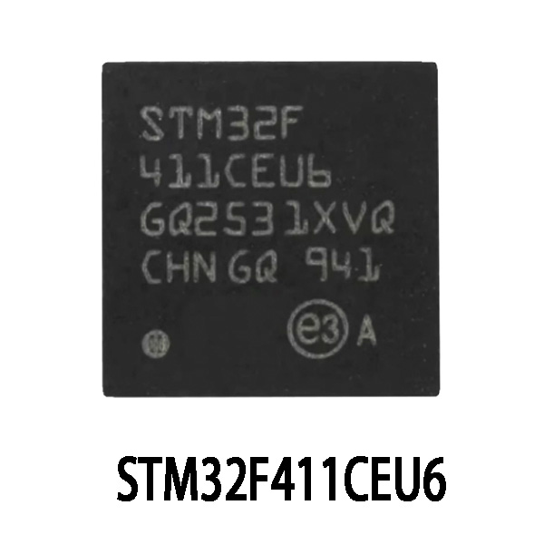


| पैरामीटर | STM32F401CCU6 | एसटीएम32F411CEU6 | STM32F103C8T6 | STM32G431CBT6 |
|---|---|---|---|---|
| Core | Cortex-M4 @ 84MHz | Cortex-M4 @ 100MHz | Cortex-M3 @ 72MHz | Cortex-M4 @ 170MHz (FPU+DSP) |
| Flash | 256 KB | 512 KB | 64 KB | 128 KB |
| SRAM | 64 KB | 128 KB | 20 KB | 32 KB |
| ADC Resolution | 12-bit (10 channels) | 12-bit (10 channels) | 12-bit (10 channels) | 12-bit (16 channels) |
| UART/USART | 3 | 3 | 3 | 4 |
| एसपीआई | 3 | 3 | 2 | 3 |
| आई2सी | 3 | 3 | 2 | 3 |
| USB Support | USB 2.0 FS Device | USB 2.0 FS Device | USB 2.0 FS Device | USB 2.0 FS Device |
| Operating Voltage | 1.8–3.6V | 1.7–3.6V | 2.0–3.6V | 1.7–3.6V |
| पैकेट | LQFP48 | LQFP48 | LQFP48 | LQFP48 |
If STM32F401CCU6 feels limited in speed or memory, you can switch directly to STM32F411CEU6. It doubles the speed and memory while staying pin-to-pin compatible. For cost-sensitive projects, STM32F103C8T6 is a popular cheaper alternative, but remember it’s Cortex-M3-based—no DSP/FPU, less memory, and CubeMX projects aren’t directly portable. Another interesting upgrade is STM32G431CBT6 from the G4 series. It’s faster, more efficient, and pin-compatible, but you’ll need to adjust or rewrite parts of your code due to architecture differences.
STM32F401CCU6 Minimum System Circuit

This schematic shows the minimal system circuit of STM32F401CCU6. It’s straightforward and suitable for beginners or mass production. The clock section has two crystals: a 25MHz for the main 84MHz system frequency and a 32.768KHz for RTC. Crystal capacitors should match your supplier’s recommendations. The BOOT0 pin uses a jumper to choose between Flash or system Bootloader startup, and NRST has a simple reset circuit with capacitor and resistor. All GPIO pins are available for easy expansion. Remember to disable the internal HSI oscillator when using an external crystal and connect PA11/PA12 properly for USB use.
STM32F401CCU6 Bootloader Wiring

From your photo, entering Bootloader mode is easy: connect BOOT0 to 3.3V using a jumper, then press reset (NRST pin). The chip will boot into system Bootloader mode, allowing you to flash firmware via USART1 (PA9/PA10) through a USB-to-serial module. The RC522 module seen in the picture uses SPI and is just for testing, not related to flashing. After flashing, move BOOT0 back to GND and reset again so your code runs properly. If you’re using ST-Link instead, you won’t even need to worry about BOOT0 settings.
STM32F401CCU6 Schematic

The STM32F401CCU6 uses an ARM Cortex-M4 core with FPU, running up to 84MHz. It’s great for signal processing and floating-point operations. With 256KB Flash and 64KB SRAM, it covers most typical applications. It supports various clock sources, including external crystals and internal RC oscillators, and the RTC has independent battery backup. Communication options are plentiful: three USARTs, three SPIs, three I²Cs, plus USB OTG FS (remember PA11/PA12 connections!). Timers and ADC (12-bit, 16 channels) offer good flexibility. Ensure you connect a capacitor to the VCAP1 pin for stable operation. Using CubeMX for pin assignment will be easy if you refer directly to the pin layout.
STM32F401CCU6 Board

The STM32F401CCU6 board you’re using is quite handy, running at 84MHz with 256K Flash and 64K RAM, suitable for most projects. It comes with a Type-C port for power and USB serial communication (using PA11/PA12 pins). Built-in SWD pins match ST-Link for easy debugging. Buttons for BOOT0 and NRST help you quickly enter Bootloader mode. The clearly marked pins like A0-A7 (PA0-PA7) simplify your connections, and the board even integrates crystals for main frequency and RTC, saving extra work. Just refer to the pin labels when setting up GPIO in CubeMX.
STM32F401CCU6 Arduino Project Usage
To start using STM32F401CCU6 with Arduino IDE, make sure your IDE version is 1.8.x or 2.x. First, add the official STM32 support URL into Arduino IDE’s preferences, and install the STM32 board package. Select “Generic STM32F4 series” and choose “BlackPill F401CCU6”. Uploading via ST-Link is easiest and most reliable, but DFU bootloader via USB or serial upload (with correct BOOT0 setting) also works. Simple examples like blinking an LED or serial communication are easy to start with. For SPI devices like the RC522 module, standard libraries usually work fine, but double-check compatibility with the F401 chip before use.
इसी तरह और भी

ZXCW6100S28
डायोड्स इन्कॉर्पोरेटेड

TDA8541T/N1,112
एनएक्सपी यूएसए इंक.

TDA8541T/N1,118
एनएक्सपी यूएसए इंक.

TDA7056B/N1,112
एनएक्सपी यूएसए इंक.
,SOT157-2.JPG "TDA2616Q/N1,112")
TDA2616Q/N1,112
एनएक्सपी यूएसए इंक.

TDA8547TS/N1,112
एनएक्सपी यूएसए इंक.
TDA8547TS/N1,118
एनएक्सपी यूएसए इंक.

NE58633BS,157
एनएक्सपी यूएसए इंक.
NE58633BS,115
एनएक्सपी यूएसए इंक.

SA58670BS,115
एनएक्सपी यूएसए इंक.

TS4961TIQT
एसटीमाइक्रोइलेक्ट्रॉनिक्स
,SOT523-1.JPG "TFA9842J/N1,112")
TFA9842J/N1,112
एनएक्सपी यूएसए इंक.
कार्ट में भी जोड़ें

BCM56851A0IFSBG
ब्रॉडकॉम लिमिटेड

LTC6655BHMS8-2.5#PBF
एनालॉग डिवाइसेज इंक.
TB6560AFG
तोशिबा

IS46TR16128A-15HBLA2
ISSI, इंटीग्रेटेड सिलिकॉन सॉल्यूशन इंक
CY8CTMG240-LQI-01T
साइप्रस सेमीकंडक्टर कॉर्प

ओपीए134यूए
बूर ब्राउन

SN75DP130DSRGZR
टेक्सास इंस्ट्रूमेंट्स

MAX7407ESA+
एनालॉग डिवाइसेज इंक./मैक्सिम इंटीग्रेटेड

MC14022BDR2G
Onsemi

TUSB321AIRWBR
टेक्सास इंस्ट्रूमेंट्स

LS6506R
LSI/CSI

FAN8841MPX
Onsemi
संबंधित उत्पाद
ZXCW6100S28
डायोड्स इन्कॉर्पोरेटेड
TDA8541T/N1,112
एनएक्सपी यूएसए इंक.
TDA8541T/N1,118
एनएक्सपी यूएसए इंक.
TDA7056B/N1,112
एनएक्सपी यूएसए इंक.
TDA2616Q/N1,112
एनएक्सपी यूएसए इंक.
TDA8547TS/N1,112
एनएक्सपी यूएसए इंक.
TDA8547TS/N1,118
एनएक्सपी यूएसए इंक.
NE58633BS,157
एनएक्सपी यूएसए इंक.
NE58633BS,115
एनएक्सपी यूएसए इंक.
SA58670BS,115
एनएक्सपी यूएसए इंक.
TS4961TIQT
एसटीमाइक्रोइलेक्ट्रॉनिक्स
TFA9842J/N1,112
एनएक्सपी यूएसए इंक.

SA58632BS,118
एनएक्सपी यूएसए इंक.

TDA1308TT/N2,118
एनएक्सपी यूएसए इंक.
TDA8552TS/N1,112
एनएक्सपी यूएसए इंक.
TDA8552TS/N1,118
एनएक्सपी यूएसए इंक.
TDA1517/N3,112
एनएक्सपी यूएसए इंक.
TDA7056A/N2,112
एनएक्सपी यूएसए इंक.

SA58671UK,027
एनएक्सपी यूएसए इंक.

TDA8948J/N1,112
एनएक्सपी यूएसए इंक.
TFA9843AJ/N1,112
एनएक्सपी यूएसए इंक.

SA58637BS,118
एनएक्सपी यूएसए इंक.

TDA7052A/N2,112
एनएक्सपी यूएसए इंक.

TDA8551T/N1,112
एनएक्सपी यूएसए इंक.

TDA8551T/N1,118
एनएक्सपी यूएसए इंक.
SA58672UK,027
एनएक्सपी यूएसए इंक.
SA58670ABS,115
एनएक्सपी यूएसए इंक.

SA58631TK,157
एनएक्सपी यूएसए इंक.
SA58631TK,118
एनएक्सपी यूएसए इंक.
SA58631TK,115
एनएक्सपी यूएसए इंक.
कृपया आरएफक्यू भेजें, हम तुरंत जवाब देंगे।
