
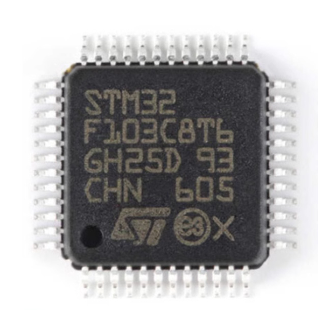
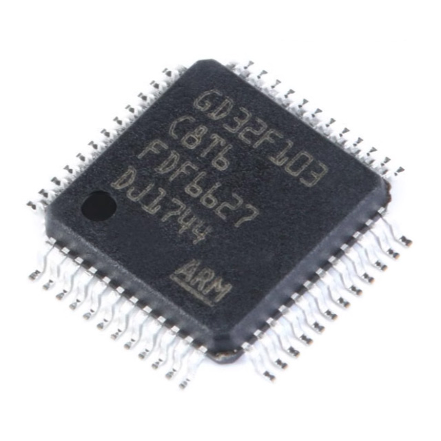
STM32F103C8T6 datasheet, pinout & VS STM32F103C6T6
- CoreProcessor: ARM® Cortex®-M3
- Core Size: 32-Bit Single-Core
- Peripherals: DMA, Motor Control PWM, PDR, POR, PVD, PWM, Temp Sensor, WDT
- Package: 48-LQFP


FREE delivery for orders over HK$250.00

Quick response, quick quotaton

Flash shipment,no worries after sales

Original channel,guarantee of the authentic products
STM32F103C8T6 BLUEPILL SSD1306 OLED DISPLAY NAVIGATION MENU (STM32 SSD1306 MENÜ TASARIMI)
STM32F103C8T6
The STM32F103C8T6 is a cost-effective 32-bit ARM Cortex-M3 microcontroller from STMicroelectronics, featuring a maximum clock speed of 72 MHz, 64KB Flash memory, and 20KB SRAM. It integrates extensive peripheral interfaces such as SPI, I²C, USART, ADC, and PWM. Thanks to its compact size, reliable performance, and mature development ecosystem, it’s widely used in industrial control systems, consumer electronics, smart home applications, and IoT devices, particularly favored by embedded system developers.
STM32F103C8T6 pinout
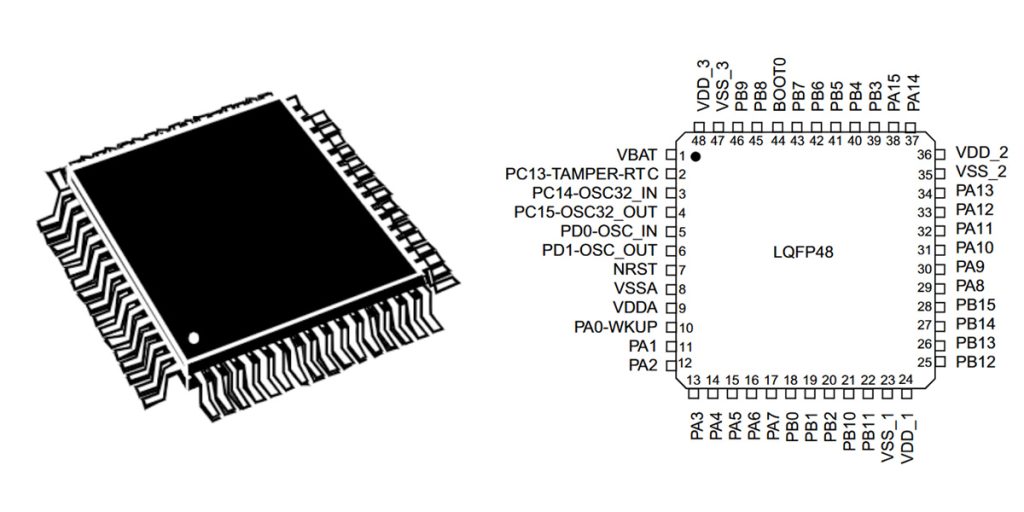
| Pin Number | Pin Name | Description |
|---|---|---|
| 1 | VBAT | Backup power supply for RTC |
| 2 | PC13-TAMPER-RTC | GPIO / RTC Tamper input / RTC output |
| 3 | PC14-OSC32_IN | GPIO / 32kHz oscillator input |
| 4 | PC15-OSC32_OUT | GPIO / 32kHz oscillator output |
| 5 | PD0-OSC_IN | GPIO / Main oscillator input |
| 6 | PD1-OSC_OUT | GPIO / Main oscillator output |
| 7 | NRST | Reset pin (active low) |
| 8 | VSSA | Analog ground |
| 9 | VDDA | Analog power supply |
| 10 | PA0 | GPIO / ADC channel / Wakeup |
| 11 | PA1 | GPIO / ADC channel |
| 12 | PA2 | GPIO / ADC channel / USART2_TX |
| 13 | PA3 | GPIO / ADC channel / USART2_RX |
| 14 | PA4 | GPIO / ADC channel / SPI1_NSS |
| 15 | PA5 | GPIO / ADC channel / SPI1_SCK |
| 16 | PA6 | GPIO / ADC channel / SPI1_MISO |
| 17 | PA7 | GPIO / ADC channel / SPI1_MOSI |
| 18 | PB0 | GPIO / ADC channel |
| 19 | PB1 | GPIO / ADC channel |
| 20 | PB2 | GPIO / Boot pin |
| 21 | PB10 | GPIO / I²C2_SCL / USART3_TX |
| 22 | PB11 | GPIO / I²C2_SDA / USART3_RX |
| 23 | VSS | Ground |
| 24 | VDD | Power supply |
| 25 | PB12 | GPIO / SPI2_NSS |
| 26 | PB13 | GPIO / SPI2_SCK |
| 27 | PB14 | GPIO / SPI2_MISO |
| 28 | PB15 | GPIO / SPI2_MOSI |
| 29 | PA8 | GPIO / USART1_CK |
| 30 | PA9 | GPIO / USART1_TX |
| 31 | PA10 | GPIO / USART1_RX |
| 32 | PA11 | GPIO / USB_DM |
| 33 | PA12 | GPIO / USB_DP |
| 34 | PA13 | GPIO / SWDIO |
| 35 | VSS | Ground |
| 36 | VDD | Power supply |
| 37 | PA14 | GPIO / SWCLK |
| 38 | PA15 | GPIO / SPI1_NSS |
| 39 | PB3 | GPIO / SPI1_SCK |
| 40 | PB4 | GPIO / SPI1_MISO |
| 41 | PB5 | GPIO / SPI1_MOSI |
| 42 | PB6 | GPIO / I²C1_SCL / TIM4_CH1 |
| 43 | PB7 | GPIO / I²C1_SDA / TIM4_CH2 |
| 44 | BOOT0 | Boot memory selection pin |
| 45 | PB8 | GPIO / TIM4_CH3 / I²C1_SCL |
| 46 | PB9 | GPIO / TIM4_CH4 / I²C1_SDA |
| 47 | VSS | Ground |
| 48 | VDD | Power supply |
STM32F103C8T6 equivalent microcontroller

| Model | Manufacturer | Clock | Flash | Package | Voltage | Notes |
|---|---|---|---|---|---|---|
| STM32F103C8T6 | STMicroelectronics | 72 MHz | 64 KB | LQFP48 | 2.0–3.6 V | Reference |
| STM32F103C6T6 | STMicroelectronics | 72 MHz | 32 KB | LQFP48 | 2.0–3.6 V | Lower memory |
| STM32F103CBT6 | STMicroelectronics | 72 MHz | 128 KB | LQFP48 | 2.0–3.6 V | More Flash |
| GD32F103C8T6 | GigaDevice | 108 MHz | 64 KB | LQFP48 | 2.6–3.6 V | Faster alt. |
| APM32F103C8T6 | Apex Microsystems | 72 MHz | 64 KB | LQFP48 | 2.0–3.6 V | Budget choice |
STM32F103C8T6 circuit wiring example

1. Main Controller
-
Utilizes the STM32F103C8T6 MCU with ARM Cortex-M3 core.
-
Clearly labeled pins show various functions, including power (VCC3V3), ground (GND), clock pins, GPIOs, and analog pins.
2. Power Supply Circuit
-
The main power input passes through a voltage regulator chip (U1), outputting a stable 3.3V for MCU operation.
-
Bypass capacitors C6 and C7 are used to stabilize and filter the power supply voltage.
3. Crystal Oscillator Circuit
-
The main oscillator is an 8 MHz crystal (Y2) paired with load capacitors C9 and C10 (20 pF each), providing a stable clock signal.
-
RTC (Real-Time Clock) uses a 32.768 kHz crystal (Y1) with load capacitors C3 and C4 for timing accuracy.
4. Reset Circuit
-
The NRST pin is pulled up to VCC3V3 via a 10 kΩ resistor (R4) to enable automatic power-on reset.
5. BOOT Configuration Circuit
-
The BOOT0 pin connects to a jumper header (Header X6) allowing the selection of boot mode:
-
Jumper position determines whether the MCU boots from internal Flash memory or system memory.
-
6. SWD Debugging Interface
-
Provides SWD interface pins (SWCLK, SWDIO) for programming and debugging.
-
Includes VCC and GND pins for easy connection to debugging tools like ST-Link.
STM32F103C8T6 uart spi i2c example
// Initialize UART (USART1)
UART_HandleTypeDef huart1;
void UART_Init(void) {
huart1.Instance = USART1;
huart1.Init.BaudRate = 9600;
huart1.Init.WordLength = UART_WORDLENGTH_8B;
huart1.Init.StopBits = UART_STOPBITS_1;
huart1.Init.Parity = UART_PARITY_NONE;
huart1.Init.Mode = UART_MODE_TX_RX;
huart1.Init.HwFlowCtl = UART_HWCONTROL_NONE;
HAL_UART_Init(&huart1);
}
int main(void) {
HAL_Init();
UART_Init();
char msg[] = “Hello\r\n”;
while (1) {
HAL_UART_Transmit(&huart1, (uint8_t*)msg, sizeof(msg)-1, HAL_MAX_DELAY);
HAL_Delay(1000);
}
}
STM32F103C8T6 arduino compatibility
The STM32F103C8T6 is highly compatible with the Arduino development environment. Users can quickly start development by installing the STM32 Arduino core, such as the official STM32duino or the community-maintained Roger Clark STM32 core. This compatibility allows you to leverage the Arduino IDE and its extensive library ecosystem, while benefiting from the powerful performance and rich peripheral interfaces of the STM32 platform. It is commonly used in IoT, robotics, and automation applications.
More Like This

MC5430F
Motorola

JD54LS51BCA
National Semiconductor

USPLSI2032VE-110LB49
Lattice Semiconductor Corporation
74S22PC
Rochester Electronics, LLC

9504DC
National Semiconductor

9005PC
National Semiconductor

9007DC
National Semiconductor
9004DC
National Semiconductor

SN74HC804DWR
Texas Instruments
SN700863DWR
Texas Instruments
4001BDMQB
National Semiconductor
54F02FMQB
National Semiconductor
Also Add to Cart
MC74HCT240AFL1
onsemi

8N3SV76EC-0061CDI8
Renesas Electronics America Inc

PAC1944T-E/J6CX
Microchip Technology

BU4811G-TR
Rohm Semiconductor

SI32171-B-GM1
Skyworks Solutions Inc.

MC74HC165D
onsemi

74ACT11240DWR
Texas Instruments
MAX9295AGTJ+E2
Analog Devices Inc./Maxim Integrated
PCF8523U/12AA/1,00
NXP USA Inc.

PI3USB40AE
Diodes Incorporated
XC6136N44C9R-G
Torex Semiconductor Ltd
ADM3101EACPZ
Analog Devices
Related Products
MC5430F
Motorola
JD54LS51BCA
National Semiconductor
USPLSI2032VE-110LB49
Lattice Semiconductor Corporation
74S22PC
Rochester Electronics, LLC
9504DC
National Semiconductor
9005PC
National Semiconductor
9007DC
National Semiconductor
9004DC
National Semiconductor
SN74HC804DWR
Texas Instruments
SN700863DWR
Texas Instruments
4001BDMQB
National Semiconductor
54F02FMQB
National Semiconductor
DM54S20W/883
National Semiconductor

MC3129L
Motorola
4071BDM
National Semiconductor
MC9814P
Motorola
MC9825P
Motorola

74AC11000NS
Texas Instruments
MC5420L
Motorola
MC5401L
Motorola
MC5401F
Motorola
SN74H61N
Texas Instruments
MC5410F
Motorola
MC5430L
Motorola

SN74AS138N-J
Texas Instruments
CD4023BCN
Fairchild Semiconductor
4019BDC
National Semiconductor
74H40DC
National Semiconductor
5420FMQB
National Semiconductor
4025BDM
National Semiconductor
Please send RFQ , we will respond immediately.
