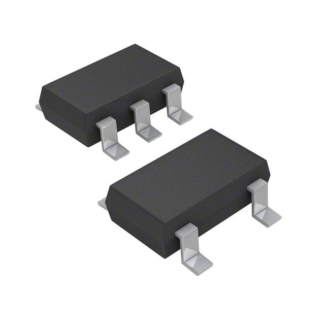
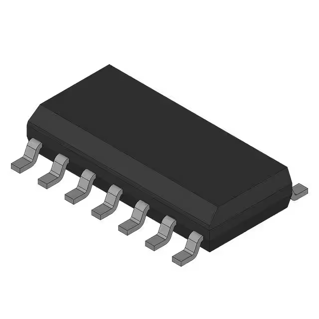
SN74LVC1G08DCKR データシート、価格、スパイスモデル
- ロジックタイプ: ANDゲート
- 回路数: 1
- 入力数: 2
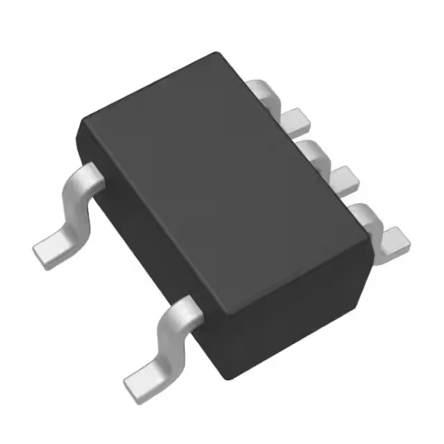
- パッケージ: SC-70-5

HK$250.00以上のご注文で送料無料

迅速な対応、迅速な見積もり

すぐに発送、アフターサービスも安心

オリジナルチャネル、本物の製品の保証
Electronics: voltage shifting from 3.3V to 1.65V with SN74LVC
sn74lvc1g08dckr
Let me walk you through why the SN74LVC1G08DCKR is such a handy little chip. At its core, it’s a single, two-input AND gate—perfect for all your basic logic needs. It handles anything from 1.65 V up to 5.5 V, so mixing different voltage levels is no sweat. Don’t worry about battery drain, either: the static current is practically zero, making it ideal for power-sensitive projects. Need speed? With just a 3.5 ns propagation delay at 3.3 V, it keeps pace with fast digital signals. And driving LEDs or small motors isn’t an issue—±24 mA output at 3.3 V gives you plenty of muscle. Built on CMOS tech, it’s resistant to noise and interference. Plus, the SC70 package is tiny, saving precious PCB real estate. Whether you’re designing a wearable gadget, communication gear, or compact industrial control, this little powerhouse has your back.
sn74lvc1g08dckr pinout diagram

| ピン番号 | ピン名 | 説明 |
|---|---|---|
| 1 | あ | AND Gate Input A |
| 2 | GND | 地面 |
| 3 | B | AND Gate Input B |
| 4 | はい | AND Gate Output Y |
| 5 | VCC | Power Supply Input (1.65~5.5V) |
Wire the A and B pins to your logic signals—only when both go high will Y output a high level. The Y pin has solid drive strength, so it can feed downstream digital loads directly. Tie VCC to a stable DC source between 1.65 V and 5.5 V, and ground GND firmly to keep noise at bay. Because it’s a CMOS part, it’s sensitive to static—ground yourself or use a wrist strap when handling. On your PCB, keep input and output traces as short as possible to minimize interference and crosstalk, ensuring clean signals. Double-check all connections before powering up to avoid mishaps.
sn74lvc1g08dckr equivalent ic

| パラメータ | SN74LVC1G08DCKR (Original) |
SN74LVC1G08DCKT | SN74LVC1G08DCKTG4 | SN74LVC1G08DCKTE4 | 74LVC1G08W5-7 |
|---|---|---|---|---|---|
| メーカー | TI | TI | TI | TI | ダイオード株式会社 |
| Logic Function | 2-input AND Gate | 2-input AND Gate | 2-input AND Gate | 2-input AND Gate | 2-input AND Gate |
| 供給電圧(V) | 1.65 – 5.5 | 1.65 – 5.5 | 1.65 – 5.5 | 1.65 – 5.5 | 1.65 – 5.5 |
| Output Drive Capability (mA) | ±32 | ±32 | ±32 | ±32 | ±32 |
| 伝播遅延(tpd) | 3.4ns @5V | 3.4ns @5V | 3.4ns @5V | 3.4ns @5V | 3.4ns @5V |
| Static Current (ICC) | 10µA | 10µA | 10µA | 10µA | 10µA |
| パッケージ | SC70-5 | SC70-5 | SC70-5 | SC70-5 | SC70-5 |
| 特徴 | Standard Version | Industrial Grade Version | Lead-free Environmental Version | Lead-free Environmental Version | TI-Compatible Alternative |
First off, make sure your replacement sits in the same SC70-5 package—same pad layout and pin order—because even if the specs match, a different footprint won’t plug in (and could fry your board). Next, double-check its voltage range, output drive, and propagation delay—tiny timing shifts can wreck high-speed logic. Though these gates sip power, if you’re on battery or packing boards tight, confirm the real power draw and heat profile stack up to or beat the original. Shipping to Europe or the US? Grab a RoHS-compliant, lead-free version (look for G4/E4 suffixes). Stick with TI or another trusted vendor—small process tweaks between makers can change performance. Don’t forget to verify stock levels and lead times so your project doesn’t stall. Finally, always run a small-batch test before swapping parts in bulk to catch any surprises early.
sn74lvc1g08dckr logic gate circuit example

this control circuit centers on a SN74LVC1G08DCKR two-input AND gate (U4815A) and a DMN74DX MOSFET (U100), both powered from a 3.3 V bus. A 0.1 µF decoupling cap on VCC keeps the supply rock-solid. Your IN signal feeds the MOSFET gate through a 10 kΩ resistor (R118), and the MOSFET’s source—via R130—drives AND pin 1. AND pin 2 grabs the PERST# line, which is smoothed by a small cap (C580) to tame noise. The AND gate’s OUT (pin 4) only goes high when both IN and PERST# are high, making it perfect for gating downstream logic or enable lines. When you pick a MOSFET, double-check its current rating and parasitic capacitance—they’ll affect signal integrity. And that’s it: simple, reliable AND logic with level shifting and noise filtering all in one.
sn74lvc1g08dckr vs sn74ahc1g08 comparison
| パラメータ | SN74LVC1G08DCKR | SN74AHC1G08 |
|---|---|---|
| Logic Function | 2-input AND Gate | 2-input AND Gate |
| Supply Voltage Range (V) | 1.65 – 5.5 | 2 – 5.5 |
| Output Current (mA) | ±32 (Strong) | ±8 (Medium) |
| 伝播遅延(tpd) | 3.4ns @5V (Faster) | 7ns @5V (Slower) |
| Static Current ICC (Typical) | 10µA | 1µA (Lower) |
| パッケージタイプ | SC70-5 | SOT-23-5, SC70-5 |
| Input Logic Level Compatibility | Supports low-voltage logic levels (1.8V, 3.3V, 5V) | Supports standard logic levels (3.3V, 5V) |
| ESD保護 | Strong (>2kV) | Medium (~2kV) |
| 推奨アプリケーション | Low-voltage, high-speed circuits, portable devices | General logic circuits, cost-effective solutions |
When you swap in an SN74AHC1G08 for the SN74LVC1G08DCKR, here’s what to watch:
-
Voltage range: The LVC handles down to 1.65 V, so it’s perfect for battery-powered or low-voltage gear. The AHC only goes down to 2 V—if you’re running under that, don’t use it.
-
Drive strength: You get ±32 mA on the LVC, so you can push LEDs or heavier logic loads. The AHC is ±8 mA—fine for light signals, but check your downstream requirements.
-
スピード: LVC’s about 3.4 ns at 5 V, great for fast buses. AHC sits around 7 ns—okay for general-purpose logic, but make sure your timing still works.
-
Quiescent current: AHC only draws ~1 µA, so it wins on standby power if ultra-low idle drain matters.
-
Input compatibility: LVC loves 1.8 V, 3.3 V, and 5 V logic. AHC is really built for 3.3 V or 5 V—double-check any lower-voltage signals.
sn74lvc1g08dckr operating voltage range
It happily runs from 1.65 V up to 5.5V. At the bottom end (1.65–1.95 V), it’s perfect for tiny, battery-powered gadgets—think wearables—where every microamp counts. You’ll see modest drive (around ±4–8 mA) and a bit more delay (5–6 ns). In the sweet spot (2.5–3.3 V), it fits right into most MCU setups like STM32, ESP32 or Raspberry Pi projects, offering about ±24 mA drive and a typical 3.5 ns delay. Crank it to 5 V, and you’ve got maximum muscle (±32 mA) with the fastest switching (~3.4 ns)—ideal for industrial control or driving LEDs and small relays. As you raise VCC, you get stronger outputs and quicker edge rates, so pick the voltage that balances power, speed, and load-driving needs for your application.
sn74lvc1g08dckr level shifting circuit
This little chip here, the SN74LVC1G08, is basically a simple logic AND gate. You feed it two input signals, and it gives you a logic output. But what’s cool about it is that it can easily help you shift signals from a higher voltage, like 5 volts, down to a lower voltage level, like 3.3 volts.
For example, if you’ve got a 5-volt signal coming from something like an Arduino and you need to safely feed it into a Raspberry Pi or an ESP32 that’s working at 3.3 volts, this chip makes it straightforward. All you need to do is power the chip at 3.3 volts, then connect your 5-volt signal into one input pin (the chip comfortably handles inputs slightly higher than its own supply voltage). The output will naturally follow the chip’s supply voltage, giving you a perfect 3.3-volt logic output.
Just remember to hook it up to ground properly, and your level shifting will work like a charm.


,SOT157-2.JPG)

,SOT523-1.JPG)

.jpg)


