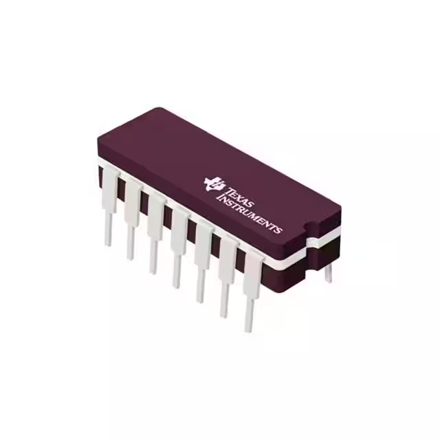
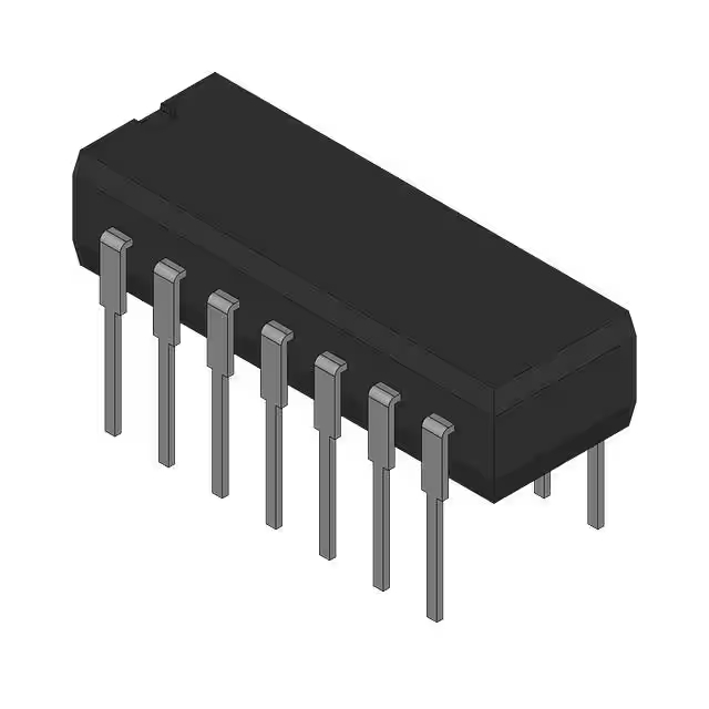
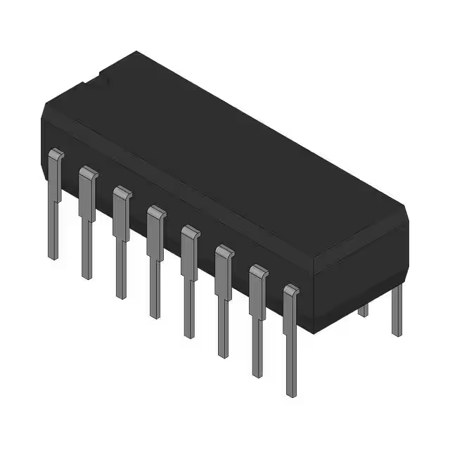
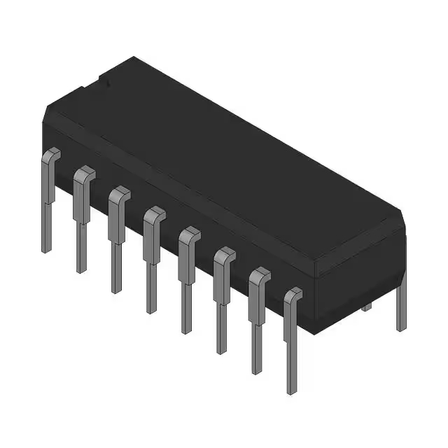
SN74HC32N datasheet, pinout & pdf
- Logic Type: OR Gate
- Number of Circuits: 4
- Number of Inputs: 2
- Package: 14-PDIP

FREE delivery for orders over HK$250.00

Quick response, quick quotaton

Flash shipment,no worries after sales

Original channel,guarantee of the authentic products
OR gate / Logische OR schakeling / SN74HC32N
sn74hc32n
The SN74HC32N is a handy quad 2-input OR gate chip that’s great for combining digital signals. It’s got four independent OR gates—basically, the output goes high whenever at least one input is high, making it perfect for combining multiple status signals or decoding addresses. It typically runs on a single 5V supply but works fine from 2V to 6V, meaning it easily fits into most digital systems, whether you’re using standard 5V or even lower-voltage setups.
You’ll notice it responds quickly (around 8 nanoseconds at 5V), so it won’t slow down your signals. It’s designed for low power, consuming minimal current—even at MHz frequencies. Plus, the outputs comfortably drive typical TTL or CMOS loads. Built-in ESD protection keeps your circuit safe from static damage, and it’s durable from –40°C to 85°C, perfect for most environments. If you’re designing logic circuits, this is a reliable, easy-to-use choice.
sn74hc32n pinout diagram

| Pin Number | Pin Name | Description |
|---|---|---|
| 1 | 1A | OR Gate 1 Input A |
| 2 | 1B | OR Gate 1 Input B |
| 3 | 1Y | OR Gate 1 Output |
| 4 | 2A | OR Gate 2 Input A |
| 5 | 2B | OR Gate 2 Input B |
| 6 | 2Y | OR Gate 2 Output |
| 7 | GND | Ground |
| 8 | 3Y | OR Gate 3 Output |
| 9 | 3A | OR Gate 3 Input A |
| 10 | 3B | OR Gate 3 Input B |
| 11 | 4Y | OR Gate 4 Output |
| 12 | 4A | OR Gate 4 Input A |
| 13 | 4B | OR Gate 4 Input B |
| 14 | VCC | Positive Power Supply (+2V to +6V, typically 5V) |
When working with the SN74HC32N chip, you’re dealing with four separate 2-input OR gates, each gate having two input pins labeled A and B, plus an output pin labeled Y. It’s crucial to feed these inputs signals within the recommended voltage, usually around 5V, to ensure clean logic-level transitions. Also, don’t leave input pins floating—always connect them to a definite high or low state.
One more thing to remember: make sure the power pin (VCC) and ground pin (GND) have solid connections. Especially the ground pin—connect it to a low-impedance ground line to reduce noise and keep your signals stable. Doing this helps your chip perform reliably and prevents strange behaviors in your circuit.
sn74hc32n equivalent ic

| Parameter / Model | SN74HC32N | CD4071BE | SN74AC32N | SN74LS32N |
|---|---|---|---|---|
| Package Type | DIP-14 | DIP-14 | DIP-14 | DIP-14 |
| Operating Voltage (V) | 2 ~ 6 | 3 ~ 15 | 2 ~ 6 | 4.75 ~ 5.25 |
| Logic Family | HC Series (CMOS) | CMOS (4000 Series) | AC Series (CMOS) | LS Series (TTL) |
| Propagation Delay (ns) | 8 ~ 15 (typical @5V) | 60 ~ 120 (typical @10V) | 5 (typical @5V) | 10 (typical @5V) |
| Logic Level Compatibility | CMOS/TTL Compatible | CMOS | CMOS/TTL Compatible | TTL |
| Output Current (mA) | ±5 | ±1.5 | ±24 | ±8 |
When you’re picking an alternative for the SN74HC32N chip, keep a close eye on voltage range and logic compatibility. For example, the CD4071BE might seem like an easy swap, but remember it has slower response times and works best in circuits running over a wider voltage range—perfect for slower or more flexible voltage systems, but maybe not the best if you’re dealing with fast signals.
On the other hand, the SN74AC32N responds quicker and can handle higher output currents, making it ideal when you need fast reaction times. Then there’s the SN74LS32N—great for old-school TTL setups, but remember its strict voltage limit around 5 volts. Before swapping, double-check your circuit’s exact voltage, logic levels, and speed needs to make sure everything runs smoothly and reliably.
sn74hc32n or gate circuit example

If you’re wondering about the difference between SN74HC32 and SN74HC32N, it’s actually pretty straightforward. Both refer to the same chip internally, but the “N” in SN74HC32N specifically means it’s in a DIP (Dual Inline Package), clearly indicating how it physically connects to your circuit board. Without the “N,” you’re looking at a generic model name without clear packaging info.
Now, let me give you an example: imagine you’re building a simple binary full adder. You’d typically feed two binary inputs (A, B) and a Carry-In signal through some XOR gates (74HC86) to calculate the Sum. For the Carry-Out, you’d combine these signals with AND gates (74HC08) and then use an SN74HC32N OR gate to check if there’s any carry-forward. So, your SN74HC32N chip neatly sums up those carry signals, clearly demonstrating how an OR gate simplifies logic in practical digital circuits.
sn74hc32n logic gate wiring
Let me show you a quick and simple way to wire up your SN74HC32N OR gate for testing. Connect pin 14 (VCC) straight to your +5V supply, and pin 7 (GND) directly to ground. Now, for your inputs, use pins 1 and 2 (1A and 1B), each connected to a switch. To avoid floating inputs, add a 10kΩ resistor from each pin to ground. Your output will come from pin 3 (1Y), going through a 220Ω resistor and an LED, then down to ground to show you clearly when the OR gate is activated.
Always make sure your power connections are solid—5 volts is perfect here—and keep the ground clean and stable to avoid strange behavior. Don’t leave inputs floating; the 10kΩ resistor trick solves that easily. And don’t forget the resistor on your LED output line—it protects your chip and the LED itself. Keep your wires neat and short to minimize noise, and handle your chip carefully to prevent static damage. This setup helps your OR gate perform reliably every time.
sn74hc32n application
The SN74HC32N OR gate is great for building practical digital logic circuits. You can use it to combine signals in scenarios like logic decision-making or checking system status—whenever you need to trigger an action if just one condition is true. It’s commonly found in digital adders (like half or full adders), especially for generating carry-out signals during binary addition.
Imagine you’re building a security alarm; you can wire multiple sensors to this chip so that if any sensor detects trouble, it immediately triggers the alarm. It’s also handy for merging several control signals into a single output.
One popular example is a full-adder circuit: XOR gates handle the basic addition, AND gates detect carry conditions, and then your OR gate neatly combines those carry conditions into a final output.
When wiring it up, keep your supply voltage stable around 5 volts and always use pull-up or pull-down resistors on inputs to avoid unexpected behavior. And remember, don’t overload its output pin beyond ±5mA to keep things reliable.
