
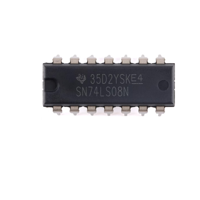
SN74LS08N datasheet, diagram, pinout, pdf
- Logic Type: AND Gate
- Number of Circuits: 4
- Number of Inputs: 2
- Package: 14-PDIP


FREE delivery for orders over HK$250.00

Quick response, quick quotaton

Flash shipment,no worries after sales

Original channel,guarantee of the authentic products
SN74LS08 | AND gate IC 7408 explanation with truth table | Two input AND gate
Sn74ls08n
If you’re working with digital logic circuits, the SN74LS08N AND gate from Texas Instruments is a solid choice. This IC gives you four 2-input AND gates, which means it can handle multiple logic operations at once. Here’s what makes it stand out:
-
Function: Each AND gate needs both inputs to be high to output a high signal. Otherwise, it outputs low. So, it’s all about ensuring both inputs match the condition.
-
Low Power: Being part of the low-power Schottky (LS) series, it consumes less power compared to regular logic chips.
-
Voltage: It runs on a 5V DC supply, with an operating voltage between 4.75V to 5.25V.
-
Output Current: The IC can drive up to 16mA of output current, perfect for connecting with other digital circuits.
-
Versatility: It’s great for TTL logic systems and works well in computers, control systems, and signal processing tasks.
This chip’s low power and reliable performance make it a great fit for various digital logic applications!
Sn74ls08n Pinout
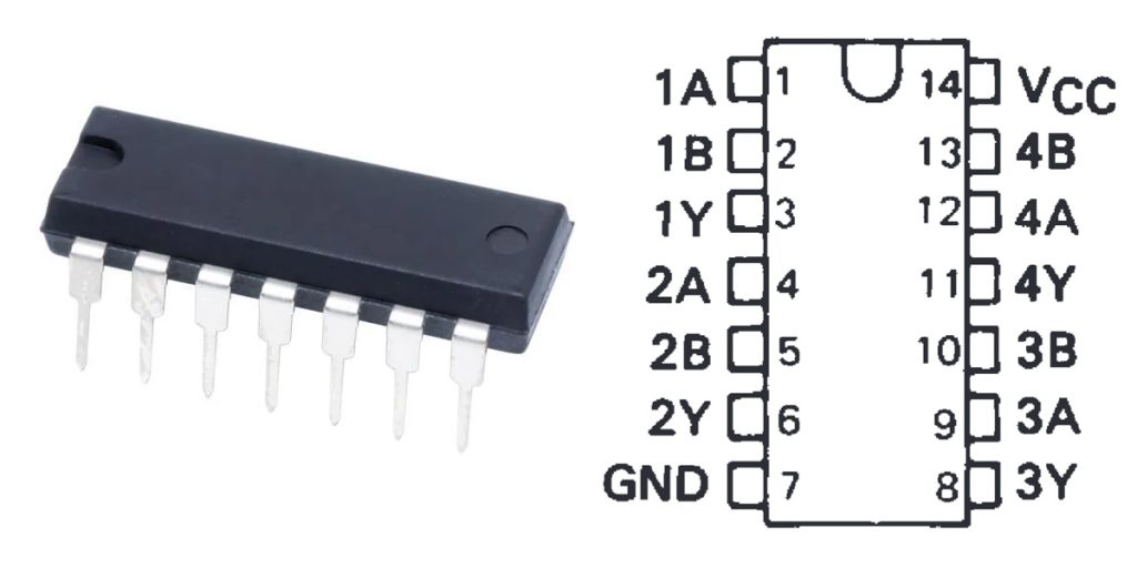
| Pin Number | Pin Name | Function Description |
|---|---|---|
| 1 | A1 | Input terminal 1, first door input |
| 2 | B1 | Input terminal 2, second door input |
| 3 | Y1 | Output terminal, first door output |
| 4 | A2 | Input terminal 1, first door input |
| 5 | B2 | Input terminal 2, second door input |
| 6 | Y2 | Output terminal, second door output |
| 7 | GND | Ground (connected to ground) |
| 8 | A3 | Input terminal 1, first door input |
| 9 | B3 | Input terminal 2, second door input |
| 10 | Y3 | Output terminal, third door output |
| 11 | A4 | Input terminal 1, first door input |
| 12 | B4 | Input terminal 2, second door input |
| 13 | Y4 | Output terminal, fourth door output |
| 14 | Vcc | Power input, connected to +5V DC power supply |
When using the SN74LS08N AND gate IC, here’s how the pinout works and what to keep in mind:
-
Inputs (A1-A4, B1-B4): These are where you connect your binary signals. Each pair of A and B inputs will determine the output based on their logic levels, so make sure they match TTL voltage levels (0V for low, 5V for high).
-
Outputs (Y1-Y4): These outputs give you the result of the logical AND operation between A and B. The output will only be high when both A and B are high.
-
GND: This pin should be connected to ground to complete the current circuit.
-
Vcc: Connect this to a 5V DC power supply to keep the IC running smoothly.
Key tips:
Make sure your power and ground pins are connected correctly for the IC to function properly. Keep the input signals within TTL levels, and don’t exceed the 16mA output current to avoid damaging the IC. Also, watch the temperature—keep it between 0°C and 70°C for optimal performance.
Sn74ls08n Equivalent Logic Gate


| Model | SN74LS08N | 74HC08N | 74HCT08N | 74LS08 |
|---|---|---|---|---|
| Package Type | DIP-14 | DIP-14 | DIP-14 | DIP-14 |
| Supply Voltage (Vcc) | 4.75V – 5.25V | 2V – 6V | 4.5V – 5.5V | 4.75V – 5.25V |
| Input Voltage (Vih/Vil) | 2V / 0.8V | 3.5V / 1.5V | 3.5V / 1.5V | 2V / 0.8V |
| Output Current (Ioh/Iol) | 8mA / 8mA | 6mA / 6mA | 6mA / 6mA | 8mA / 8mA |
| Operating Temperature Range | -40°C to +85°C | -40°C to +125°C | -40°C to +125°C | -40°C to +85°C |
| Logic Family | TTL | CMOS | CMOS / TTL | TTL |
| Special Features | Standard four-input gates | High-speed CMOS four-input gates | TTL compatible CMOS four-input gates | Standard four-input gates |
When choosing a replacement for the SN74LS08N, here are a few things to consider:
-
Power Supply Voltage (Vcc): Different models support different voltage ranges. For example, the 74HC08N has a wider voltage range (2V to 6V), which makes it more versatile for various applications. Make sure the voltage range matches your system needs.
-
Input Voltage Compatibility: The 74HC08N and 74HCT08N are CMOS series and can work with TTL circuits, while the 74LS08N is TTL-based. If you need higher compatibility, the 74HCT08N might be the better choice.
-
Output Current: There are slight differences in output current across models. For standard loads, any model will work fine. But for specific applications, choosing the model with the right output current is ideal.
-
Temperature Range: The 74HC08N and 74HCT08N have a wider temperature range (-40°C to +125°C), making them suitable for more demanding environments. Pick a model that fits your temperature needs.
-
Package Compatibility: All models come in a DIP-14 package, so they’re easy to swap without worrying about compatibility.
Sn74ls08n and Gate Circuit Diagram
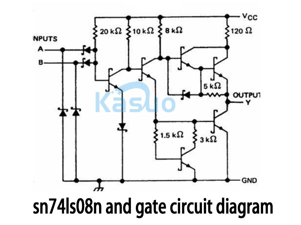
This circuit uses the SN74LS08N IC, which contains four 2-input AND gates. Each gate takes in two signals and outputs the logical AND result.
The inputs A and B represent the two signals you’re working with. These signals pass through resistors and diodes, which help adjust the voltage and protect the circuit from issues like high voltage or reverse current.
The resistors in the circuit, such as 20 kΩ, 10 kΩ, 8 kΩ, and others, control the current to keep everything running smoothly. The 5 kΩ resistor at the output helps limit current to protect the IC.
The output Y is where the result of the AND operation comes out. The output is high (1) only when both inputs A and B are high. If either input is low (0), the output will be low.
The circuit gets its power from Vcc (usually 5V), and GND is the ground to keep everything stable.
Sn74ls08n Logic Gate Ic Application
The SN74LS08N is a widely used TTL AND gate IC that features four independent 2-input AND gates. It’s perfect for a variety of digital logic applications, like performing basic AND operations in circuits. For example, it outputs high only when both inputs are high. You can use this IC to design more complex logic circuits like adders, subtracters, and decoders. It’s also useful in control circuits, where it can manage multiple signals. For instance, it will activate something like a motor or relay only when multiple conditions are met. It’s great for signal processing too, like filtering out noise and ensuring stable signals. Additionally, it plays a role in timing and synchronization, helping combine clock signals to ensure everything is in sync. Whether you’re working with computers, embedded systems, or security setups, this IC helps handle multiple inputs and triggers actions only when necessary, making it a reliable component in various circuits.
Sn74ls08n Ttl Logic Level Specs
| Parameter | Value |
|---|---|
| Input High Voltage (Vih) | 2V (min) |
| Input Low Voltage (Vil) | 0.8V (max) |
| Output High Voltage (Voh) | 2.4V (min) at Ioh = -400 µA |
| Output Low Voltage (Vol) | 0.4V (max) at Iol = 8 mA |
| Input Current (Iin) | 40 µA (max) at Vcc = 5V |
| Output Current (Ioh/Iol) | -400 µA (max) / 8 mA (max) |
| Operating Voltage (Vcc) | 4.75V to 5.25V |
| Propagation Delay (tpd) | 10 ns (typ) |
| Power Supply Current (Ic) | 4 mA (typ) at Vcc = 5V |
| Temperature Range (Operating) | -40°C to +85°C |
| Power Dissipation (Pd) | 500 mW (max) |
When you’re working with the SN74LS08N AND gate IC, here are some key voltage levels and current specs to keep in mind. First, Vih is the minimum voltage required for the input to be recognized as a logical “1”—for this IC, it’s 2V. On the flip side, Vil is the maximum voltage considered a logical “0” at the input, which is 0.8V. For the output, Voh is the minimum voltage when the output is high, which is 2.4V at a typical output current of -400 µA. Vol, the maximum voltage for a low output, is 0.4V at a typical current of 8 mA. The input current is pretty low, maxing out at 40 µA, while the output current can go up to 8 mA for low-level output and -400 µA for high-level output. This IC operates within a 4.75V to 5.25V range, which is standard for TTL logic circuits, making it easy to integrate with other TTL or CMOS components.
Sn74ls08n Input and Output Voltage
When working with the SN74LS08N TTL logic AND gate IC, understanding the input and output voltage levels is key. For the input, the voltage needs to be above 2V to be recognized as a logic high (1), and it should not exceed 0.8V to be considered a logic low (0). For the output, when it’s high (logic 1), the voltage will be at least 2.4V with a typical current of -400 µA. When it’s low (logic 0), the voltage will not exceed 0.4V with a typical current of 8 mA. These voltage levels ensure the IC operates according to TTL standards, making it compatible with other TTL logic circuits. The SN74LS08N runs on a 5V supply (from 4.75V to 5.25V), which is standard for TTL ICs, ensuring reliable communication with other components in your system.
Sn74ls08n Digital Circuit Example
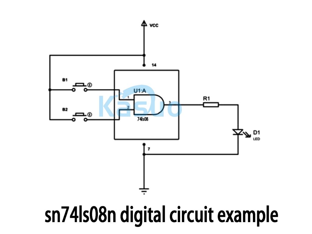
In this circuit, you’re using the SN74LS08N AND gate IC, which has two inputs. The inputs are connected to two buttons, B1 and B2. When you press a button, it sends a high signal (1), and when you release it, it sends a low signal (0). Each input has a pull-down resistor to make sure the input is in a known state. Now, the output is connected to an LED through a resistor, and the LED’s state depends on the AND gate’s output. Here’s how it works: when both buttons are not pressed (both inputs are low), the output is low, and the LED stays off. If one button is pressed, the output is still low, and the LED remains off. But, when both buttons are pressed at the same time, both inputs are high, and the output becomes high, which turns the LED on. It’s a simple yet effective example of using an AND gate to require multiple conditions to trigger an action.
Sn74ls08n Ic Wiring With Arduino
To connect the SN74LS08N IC to your Arduino, you’ll need to wire it up correctly for logical operations. Start by connecting the Vcc pin of the IC to the 5V pin on the Arduino and the GND pin of the IC to the GND on the Arduino. For inputs, connect the pins of the IC (like Pin 1 and Pin 2) to digital pins on the Arduino (for example, Pin 2 and Pin 3). You can use push buttons between the pins and GND to simulate the inputs, and don’t forget to add pull-down resistors to keep the inputs low when the buttons aren’t pressed. For the output, wire the IC’s output pin (e.g., Pin 3) to an LED with a current-limiting resistor to visualize the result. Alternatively, you can connect the output to another digital pin on the Arduino for use in your code. In your code, check the states of the inputs, and if both are HIGH, the output pin will also be HIGH, lighting up the LED.
More Like This

MC5430F
Motorola

JD54LS51BCA
National Semiconductor

USPLSI2032VE-110LB49
Lattice Semiconductor Corporation
74S22PC
Rochester Electronics, LLC

9504DC
National Semiconductor

9005PC
National Semiconductor

9007DC
National Semiconductor
9004DC
National Semiconductor

SN74HC804DWR
Texas Instruments
SN700863DWR
Texas Instruments
4001BDMQB
National Semiconductor
54F02FMQB
National Semiconductor
Also Add to Cart

74HC4094N,652
NXP USA Inc.

KSZ8001LI
Microchip Technology

LTC3245IDE#PBF
Analog Devices Inc.

M74HC221RM13TR
STMicroelectronics

TS3V330DGVR
Texas Instruments

MXD1818UR29+T
Analog Devices Inc./Maxim Integrated

AD7868AR-REEL
Analog Devices Inc.

MM3474F04VBE
Mitsumi Electric Company Ltd

BD88400FJ-GE2
Rohm Semiconductor

CS8405A-CS
Cirrus Logic Inc.

AY0438/P
Microchip Technology

SI53350BD12748-AMR
Skyworks Solutions Inc.
Related Products
MC5430F
Motorola
JD54LS51BCA
National Semiconductor
USPLSI2032VE-110LB49
Lattice Semiconductor Corporation
74S22PC
Rochester Electronics, LLC
9504DC
National Semiconductor
9005PC
National Semiconductor
9007DC
National Semiconductor
9004DC
National Semiconductor
SN74HC804DWR
Texas Instruments
SN700863DWR
Texas Instruments
4001BDMQB
National Semiconductor
54F02FMQB
National Semiconductor
DM54S20W/883
National Semiconductor

MC3129L
Motorola
4071BDM
National Semiconductor
MC9814P
Motorola
MC9825P
Motorola

74AC11000NS
Texas Instruments
MC5420L
Motorola
MC5401L
Motorola
MC5401F
Motorola
SN74H61N
Texas Instruments
MC5410F
Motorola
MC5430L
Motorola

SN74AS138N-J
Texas Instruments
CD4023BCN
Fairchild Semiconductor
4019BDC
National Semiconductor
74H40DC
National Semiconductor
5420FMQB
National Semiconductor
4025BDM
National Semiconductor
Please send RFQ , we will respond immediately.
