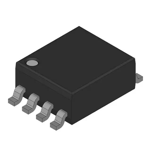
SN74LVC1G125DCK datasheet, pdf
- Brands: Texas Instruments
- Download: -
- Price: inquiry
- In Stock: 10986
- Supply Current - Max: 10 uA
- Logic Type: CMOS
- Output Type: 3-State
- Package: SC70-5

FREE delivery for orders over HK$250.00

Quick response, quick quotaton

Flash shipment,no worries after sales

Original channel,guarantee of the authentic products
sn74lvc1g125dck
If you’re working with low-voltage systems, the SN74LVC1G125DCK is a great choice. It’s a single bus buffer/driver that isolates the driving signal from the rest of the circuit. It supports both 3.3V and 5V logic levels, perfect for modern digital systems. With a fast switching speed and tri-state output, it’s ideal for bus systems where multiple drivers share the same line. Plus, it operates at a wide voltage range (2.0V to 5.5V) and has low power consumption, making it great for battery-powered designs. It comes in a small SC-70 package, saving space in tight applications.
sn74lvc1g125dck pinout diagram
| Pin Number | Pin Name | Description |
|---|---|---|
| 1 | A | Input (Data Input to the Buffer) |
| 2 | OE | Output Enable (Controls the output state, active low) |
| 3 | Y | Output (Buffered Output) |
| 4 | GND | Ground |
| 5 | VCC | Power Supply (3.3V to 5.5V) |
Here’s a quick breakdown of the pinout:
-
Pin 1 (A): This is the input pin. The signal here will be passed to the output (Pin 3), as long as the OE pin is active.
-
Pin 2 (OE): The Output Enable pin controls whether the buffer is active. If OE is low, the signal from Pin A will appear on Pin Y. If OE is high, the output is in a high-impedance state, effectively disconnecting it.
-
Pin 3 (Y): This is the output pin, where the buffered signal is sent.
-
Pin 4 (GND): Connect this to ground.
-
Pin 5 (VCC): Power supply pin. Connect it to a 3.3V to 5.5V power source.
Make sure OE is low to pass the signal through. Keep the power supply in the recommended range for proper function.
sn74lvc1g125dck equivalent buffer ic
| Model | SN74LVC1G125DCK | SN74LVC1G126DCK | NC7S125P5X | LVC1G125DCK |
|---|---|---|---|---|
| Package | SC-70 (DCK) | SC-70 (DCK) | SC-70 (P5X) | SC-70 (DCK) |
| Operating Voltage | 2.0V to 5.5V | 2.0V to 5.5V | 1.65V to 5.5V | 2.0V to 5.5V |
| Input Voltage | VCC | VCC | VCC | VCC |
| Output Voltage | VCC | VCC | VCC | VCC |
| Output Type | Tri-state | Tri-state | Tri-state | Tri-state |
| Propagation Delay | 3.0ns (typical) | 3.2ns (typical) | 3.5ns (typical) | 2.8ns (typical) |
| Pin Count | 5 pins | 5 pins | 5 pins | 5 pins |
| Additional Notes | Popular for low-voltage, high-speed logic systems | Active-low output enable (OE) | Faster switching, lower voltage range | Lower propagation delay, same functionality |
The SN74LVC1G125DCK and SN74LVC1G126DCK are quite similar, but the 126 model has an active-low output enable (OE), which works well if you need an inverted OE for your design.
The NC7S125P5X is great for low-voltage designs, with a voltage range as low as 1.65V, but it does have a slightly higher propagation delay compared to the others.
For the fastest switching, the LVC1G125DCK is your best bet with a super low propagation delay of just 2.8ns, making it ideal for high-speed applications.
If your design runs below 2V, go with the NC7S125P5X. If speed is key, choose the LVC1G125DCK.
sn74lvc1g125dck enable pin circuit

This schematic shows how to use the SN74LVC1G125DCK buffer IC with the /OE (Output Enable) pin. Here’s the rundown:
-
Pin 1 (/OE): Controls the output. When /OE is low, the signal from A goes to Y. When /OE is high, Y is in a high-impedance state (basically disconnected).
-
Pin 3 (A): Input signal.
-
Pin 5 (Y): Buffered output.
-
Capacitor (C19): This helps filter or stabilize the signal.
-
Resistor (R18): Pulls the output to a specific state or limits current when the output is disabled.
The /OE pin is key when you’re sharing a bus with multiple devices to avoid interference.
sn74lvc1g125dck logic level buffer wiring、
To set up the SN74LVC1G125DCK as a logic level buffer, here’s what you need to do:
-
Pin 1 (OE): Connect this to ground (GND) or a control signal. When OE is low, the output is enabled.
-
Pin 2 (GND): Connect to ground.
-
Pin 3 (A): This is where you connect your input signal.
-
Pin 4 (VCC): Connect this to your power supply, either 3.3V or 5V.
-
Pin 5 (Y): This is the buffered output.
OE Pin: Pull OE low to enable the output. If you pull it high, the output goes into a high-impedance state, disconnecting it from the circuit.
For extra stability, you can add a pull-up resistor (10kΩ) on Y or a 0.1µF capacitor between VCC and GND to reduce noise.
sn74lvc1g125dck smd logic driver usage
The SN74LVC1G125DCK is a handy SMD logic driver with a tri-state output. It helps isolate signals or shift logic levels between devices with different voltage requirements. For example, it’s great for preventing bus contention when multiple devices share the same communication lines.
-
The /OE pin lets you control when the output is active or in a high-impedance state.
-
It works with 2.0V to 5.5V and has a low propagation delay of around 3.0ns.
-
It’s perfect for applications where you need signal buffering, level shifting, or managing high-speed data transmission.
This IC is compact, low-power, and works well for low-voltage systems, making it ideal for projects where space is tight.
sn74lvc1g125dck io interface project
If you’re working on a project where you need to connect a 5V microcontroller to a 3.3V sensor, the SN74LVC1G125DCK buffer is a great solution. It helps you level shift and isolate the signals between the two.
Here’s how it works: Connect the OE pin to GND to enable the output. Pin A gets the input from the MCU, while Pin Y sends the buffered signal to the sensor. With VCC at 3.3V, the buffer ensures the sensor gets the right voltage without any issues.
In your code, you’ll send data from the microcontroller and read the sensor data through the buffer.


