
XCF04SVOG20C datasheet & replacement | dimension
- Brands: AMD Xilinx
- Download: -
- Price: inquiry
- In Stock: 7596
- Product Status: Obsolete
- Programmable Type: In System Programmable
- Memory Size: 4Mb
- Package: 20-TSSOP (0.173, 4.40mm Width)


FREE delivery for orders over HK$250.00

Quick response, quick quotaton

Flash shipment,no worries after sales

Original channel,guarantee of the authentic products
xcf04svog20c
If you’re looking at the XCF04SVOG20C configuration memory chip, here’s what you need to know. It offers 4Mb (512KB) of storage, runs comfortably between 3.0V to 3.6V (typically 3.3V), and comes in a compact 20-pin TSSOP package, which is perfect for tight PCB layouts.
It’s built tough, designed to handle industrial conditions from -40°C up to +85°C, making it ideal for industrial control, automotive electronics, and communication gear. With a reliable lifespan of 20,000 program cycles and data retention of at least 20 years, you can count on its durability. It supports both serial and parallel interfaces, and you can program it right in your system via JTAG, simplifying your setup and testing.
However, keep in mind it’s been discontinued. For new designs, you’ll probably want to look at modern alternatives like AMD’s XCFxxP series or similar chips from other manufacturers.
xcf04svog20c pinout configuration
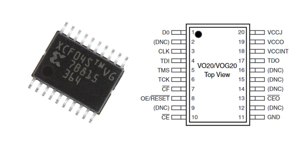
| Pin Number | Pin Name | Description |
|---|---|---|
| 1 | D0 | Data Output (DATA) |
| 2 | CLK | Configuration Clock Input (CCLK) |
| 3 | OE/RESET | Output Enable/Reset Control |
| 4 | CE | Chip Enable (Active Low) |
| 5 | TDI | JTAG Data Input |
| 6 | TMS | JTAG Mode Select |
| 7 | TCK | JTAG Clock Input |
| 8 | TDO | JTAG Data Output |
| 9 | VCCINT | Internal Power Supply Input (3.3V) |
| 10 | VCCO | I/O Power Supply Input (1.8-3.3V) |
| 11 | VCCJ | JTAG I/O Power Supply Input (2.5-3.3V) |
| 12 | GND | Ground |
| 13~20 | NC | No Connection |
When wiring up your chip, there are a few things you’ll want to pay attention to. First, make sure you provide a stable 3.3V supply for VCCINT—adding a decoupling capacitor nearby will help keep the voltage clean. For the I/O voltage (VCCO), match it to your connected FPGA or other peripherals, typically between 1.8V and 3.3V. Also, ensure your JTAG voltage (VCCJ) aligns with your programmer, usually 2.5V to 3.3V.
Speaking of JTAG pins (TDI, TMS, TCK, TDO), keep these lines short and free from interference to avoid signal issues. If you’re not using JTAG, make sure these pins aren’t left floating—ground them or handle them appropriately.
For control pins like OE/RESET and CE, always set clear and stable logic levels to prevent unexpected triggering. Lastly, leave unused pins unconnected to avoid accidental interference. Remember, a good grounding plane and proper decoupling around the chip are key for stable, reliable performance.
xcf04svog20c equivalent fpga configuration

| Parameter | XCF04SVOG20C | XCF02SVOG20C | XCF01SVOG20C | EPCQ4ASI8N |
|---|---|---|---|---|
| Memory Capacity | 4 Mb | 2 Mb | 1 Mb | 4 Mb |
| Operating Voltage | 3.0~3.6 V | 3.0~3.6 V | 3.0~3.6 V | 2.7~3.6 V |
| Package Type | 20-TSSOP | 20-TSSOP | 20-TSSOP | 8-SOIC |
| Configuration Mode | Master/Slave Serial | Master/Slave Serial | Master/Slave Serial | Active Serial |
| Supply Status | Obsolete | Obsolete | Obsolete | Active |
| Remarks | Original part number | Half memory capacity | Reduced memory capacity | Altera/Intel FPGA configuration chip |
When you’re picking a replacement chip for your FPGA configuration, here are some key points you’ll want to keep in mind. First, always check that the new chip has enough storage capacity for your FPGA’s bitstream—you definitely don’t want to run short.
Next, make sure the replacement’s voltage levels match your original design exactly; otherwise, your setup might act unpredictably. It’s best to stick with the same package type if you can, to avoid redesigning your PCB. Remember, switching to something like EPCQ4ASI8N, which has a different package, means you’ll need to redo your layout.
Also, the configuration mode must be compatible with your existing setup—whether it’s Master, Slave, or Active—to ensure smooth operation. Lastly, since the original XCF series is largely discontinued, pick a chip that’s easy to source long-term, like EPCQ4ASI8N or another stable alternative, to save yourself future headaches.
xcf04svog20c fpga programming circuit
If you’re using the XCF04SVOG20C to program your FPGA, here’s how you can set it up easily. This chip stores the FPGA’s configuration bitstream, automatically feeding it to the FPGA when powered up—making your FPGA ready to go.
First, program the PROM using the JTAG interface—hook up your programmer to the TDI, TDO, TMS, and TCK pins. Once powered, the PROM sends the bitstream data from its D0 pin to the FPGA’s DIN pin. The FPGA generates a clock (CCLK), syncing data transfer smoothly.
Make sure the OE/RESET pin is FPGA-controlled for reliable data handling, and connect the CE pin to ground or control logic. Provide a stable 3.3V power source to VCCINT, VCCO, and VCCJ pins, with proper grounding.
Keep your JTAG and data lines short and noise-free. Properly handle unused pins and ensure stable power filtering to maintain reliable, interference-free FPGA configuration.
xcf04svog20c jtag wiring example
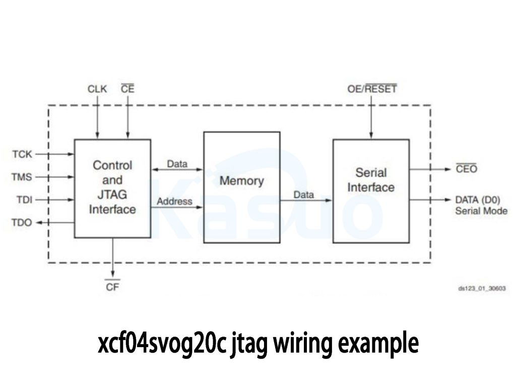
| PROM Chip Pin | Function | Connected to (JTAG Programmer) |
|---|---|---|
| TCK | Clock Input | TCK |
| TMS | Mode Select | TMS |
| TDI | Data Input | TDO (Programmer) |
| TDO | Data Output | TDI (Programmer) |
If you’re setting up your FPGA with a JTAG connection, here’s a quick rundown on how it works. The JTAG interface helps you configure, program, and debug your FPGA or PROM chips. You’ll connect four main pins: TCK (clock), TMS (mode selection), TDI (data going into the PROM), and TDO (data coming out for verification).
When wiring things up, link the TCK, TMS, TDI, and TDO pins directly between your programmer (like the Xilinx Platform Cable USB II) and your PROM chip, ensuring a solid ground connection to keep signals clean.
Keep your cables short to avoid signal degradation, and route the TCK line away from noisy areas to minimize interference. Double-check your 3.3V power source is stable before starting.
Finally, use programming software like Xilinx iMPACT or Vivado to upload and verify your FPGA’s configuration bitstream, ensuring everything is programmed correctly and running smoothly.
xcf04svog20c spi interface example
The XCF04SVOG20C is a handy Flash PROM from Xilinx (now part of AMD), designed specifically to store and feed configuration data to your FPGA. It has a storage capacity of 4Mb and uses Xilinx’s own serial interface, which feels a bit like SPI but isn’t exactly the same.
When wiring it up, your PROM’s D0 pin sends data straight into your FPGA’s DIN pin, with the CLK pin syncing up with the FPGA’s CCLK line. Your FPGA typically controls the OE/RESET pin to manage data flow and prevent interference, while the CE pin is usually grounded or FPGA-managed.
Make sure voltage levels match between your FPGA and the PROM, typically within 1.8V to 3.3V. Keep your data and clock lines short and neat on your PCB to maintain clean signals, and don’t forget a decoupling capacitor near the power pins for stability.
xcf04svog20c fpga bootloader application
If you’re using the XCF04SVOG20C chip, think of it as your FPGA’s personal bootloader. It stores the essential bitstream data your FPGA needs to kick-start properly. When your FPGA powers up, it sends out a clock signal (CCLK), prompting the XCF04SVOG20C to deliver the stored data directly to the FPGA via its data pin (D0).
For a smooth setup, first load your FPGA bitstream onto the XCF04SVOG20C using tools like Xilinx Vivado or iMPACT. Always ensure voltage levels match—typically around 3.3V—to avoid issues. Control the OE/RESET pin properly if your design requires temporarily stopping data flow.
Keep your PCB routes short and direct, especially for the data and clock signals, to prevent noise and delays. Lastly, include decoupling capacitors near the PROM’s power pins to maintain stable, clean power, ensuring reliable startup every time.
More Like This

APX809-44SAG-7
Diodes Incorporated

ADM1063ACPZ
Analog Devices Inc.

ADM1062ASUZ
Analog Devices Inc.

MAX16031ETM+
Analog Devices Inc./Maxim Integrated

MAX814KCSA+
Analog Devices Inc./Maxim Integrated

ADM1062ACPZ-REEL7
Analog Devices Inc.

MAX693EPE+
Analog Devices Inc./Maxim Integrated

MAX6884ETP+
Analog Devices Inc./Maxim Integrated

MAX791ESE+
Analog Devices Inc./Maxim Integrated

LTC2936IGN#PBF
Analog Devices Inc.

LTC695ISW-3.3#PBF
Analog Devices Inc.
ADM1062ASUZ-REEL7
Analog Devices Inc.
Also Add to Cart

FAN6250M6X
onsemi

EPM7064SLC84-6
Intel

ADR381ARTZ-REEL7
Analog Devices Inc.

5CSE-L2-3Y8-RC
Critical Link LLC

THCV219
THine Solutions, Inc.

LPC11U24FBD48/301
NXP USA Inc.

PAL16R8B2CNL
Vantis

MC14040BDR2
onsemi

ISL9519QHRTZ
Renesas Electronics America Inc

HC4P5509B-5
Harris Corporation

APM32F103C8T6
Geehy

MAX6720UTTID3
Analog Devices Inc./Maxim Integrated
Related Products
APX809-44SAG-7
Diodes Incorporated
ADM1063ACPZ
Analog Devices Inc.
ADM1062ASUZ
Analog Devices Inc.
MAX16031ETM+
Analog Devices Inc./Maxim Integrated
MAX814KCSA+
Analog Devices Inc./Maxim Integrated
ADM1062ACPZ-REEL7
Analog Devices Inc.
MAX693EPE+
Analog Devices Inc./Maxim Integrated
MAX6884ETP+
Analog Devices Inc./Maxim Integrated
MAX791ESE+
Analog Devices Inc./Maxim Integrated
LTC2936IGN#PBF
Analog Devices Inc.
LTC695ISW-3.3#PBF
Analog Devices Inc.
ADM1062ASUZ-REEL7
Analog Devices Inc.
MAX693AESE+
Analog Devices Inc./Maxim Integrated
MAX795TCSA+
Analog Devices Inc./Maxim Integrated

LTC2936CUFD#PBF
Analog Devices Inc.

LTC2936CGN#PBF
Analog Devices Inc.
MAX692AESA+
Analog Devices Inc./Maxim Integrated

LTC695CSW-3.3#PBF
Analog Devices Inc.
MAX690AESA+
Analog Devices Inc./Maxim Integrated

LTC2914IDHC-2#PBF
Analog Devices Inc.

ADM1068ASTZ
Analog Devices Inc.
LTC2914HDHC-2#PBF
Analog Devices Inc.
DS1706LESA+
Analog Devices Inc./Maxim Integrated
ADM1069ASTZ
Analog Devices Inc.

MAX691EWE+
Analog Devices Inc./Maxim Integrated
MAX690SCSA+
Analog Devices Inc./Maxim Integrated
ADM1065ASUZ-RL7
Analog Devices Inc.
LTC2914CDHC-1#PBF
Analog Devices Inc.

LTC2914CGN-2#PBF
Analog Devices Inc.

MAX818LCPA+
Analog Devices Inc./Maxim Integrated
Please send RFQ , we will respond immediately.
