The STM32F411CEU6 chip is pretty impressive. If you’re working on smart wearables, robotic controllers, or portable IoT gadgets, this one’s a great pick. It runs on an ARM Cortex-M4 core at up to 100MHz, so it handles data quickly and smoothly. With 512KB of flash and 128KB of SRAM, there’s plenty of memory for complex algorithms. Plus, it has an integrated FPU, boosting math operations—great for digital signal processing and real-time control. You’ll find useful peripherals like USB OTG, SPI, I²C, USART, and multiple ADC channels. All that with low power consumption, strong performance, and an affordable price, giving you excellent value.

STM32F411CEU6 | Arduino & datasheet
Explore the STM32F411CEU6 for Arduino projects with its powerful features. Access the Datasheet to review specifications, pin configurations, and technical details for seamless integration and efficient development.
- Бренды: STMicroelectronics
- Скачать: STM32F411CEU6 Datasheet PDF
- Цена: расследование
- В наличии: 21,002
- CoreПроцессор: ARM® Cortex®-M4
- Размер ядра: 32-битный одноядерный
- Периферийные устройства: Обнаружение/сброс отключения питания, DMA, I²S, POR, PWM, WDT
- Упаковка: 48-UFQFN Открытая прокладка


БЕСПЛАТНАЯ доставка для заказов свыше HK$250.00

Быстрый ответ, быстрая расценка

Быстрая отправка, никаких проблем после продажи

Оригинальный канал, гарантия подлинности продукции
Getting Started with the Black Pill Arduino STM32F4
STM32F411CEU6
STM32F411CEU6 Pinout Diagram

| Номер контакта | Имя пин-кода | Тип | Описание |
|---|---|---|---|
| 1 | ВССА | Власть | Аналоговое заземление |
| 2 | ВДДА | Власть | Analog Power Supply (typically 3.3V) |
| 3 | ПА0 | Ввод/вывод | GPIO, ADC_IN0, TIM2_CH1, USART2_CTS, etc. |
| 4 | ПА1 | Ввод/вывод | GPIO, ADC_IN1, TIM2_CH2, USART2_RTS, etc. |
| 5 | ПА2 | Ввод/вывод | GPIO, ADC_IN2, TIM2_CH3, USART2_TX |
| 6 | ПА3 | Ввод/вывод | GPIO, ADC_IN3, TIM2_CH4, USART2_RX |
| 7 | ПА4 | Ввод/вывод | GPIO, ADC_IN4, SPI1_NSS, USART2_CK |
| 8 | ПА5 | Ввод/вывод | GPIO, ADC_IN5, SPI1_SCK, TIM2_CH1 |
| 9 | ПА6 | Ввод/вывод | GPIO, ADC_IN6, SPI1_MISO, TIM3_CH1 |
| 10 | ПА7 | Ввод/вывод | GPIO, ADC_IN7, SPI1_MOSI, TIM3_CH2 |
| 11 | ПБ0 | Ввод/вывод | GPIO, ADC_IN8, TIM3_CH3 |
| 12 | ПБ1 | Ввод/вывод | GPIO, ADC_IN9, TIM3_CH4 |
| 13 | ПБ2 | Ввод/вывод | GPIO, BOOT1 |
| 14 | НРСТ | Вход | Reset Pin |
| 15 | ВСС | Власть | Цифровая земля |
| 16 | ВДД | Власть | Digital Power Supply (typically 3.3V) |
| 17 | ПА8 | Ввод/вывод | GPIO, MCO, TIM1_CH1 |
| 18 | ПА9 | Ввод/вывод | GPIO, USART1_TX, TIM1_CH2 |
| 19 | ПА10 | Ввод/вывод | GPIO, USART1_RX, TIM1_CH3 |
| 20 | ПА11 | Ввод/вывод | GPIO, USB_DM, TIM1_CH4 |
| 21 | ПА12 | Ввод/вывод | GPIO, USB_DP, TIM1_ETR |
| 22 | ПА13 | I/O/SWDIO | Debug Interface SWDIO |
| 23 | ПА14 | I/O/SWCLK | Debug Interface SWCLK |
| 24 | ПА15 | Ввод/вывод | GPIO, SPI1_NSS, TIM2_CH1 |
| 25 | ПБ3 | Ввод/вывод | GPIO, SPI1_SCK, TIM2_CH2, TRACESWO |
| 26 | ПБ4 | Ввод/вывод | GPIO, SPI1_MISO, TIM3_CH1 |
| 27 | ПБ5 | Ввод/вывод | GPIO, SPI1_MOSI, I2C1_SMBA |
| 28 | ПБ6 | Ввод/вывод | GPIO, I2C1_SCL, USART1_TX, TIM4_CH1 |
| 29 | ПБ7 | Ввод/вывод | GPIO, I2C1_SDA, USART1_RX, TIM4_CH2 |
| 30 | BOOT0 | Вход | Boot Selection Pin |
| 31 | ПБ8 | Ввод/вывод | GPIO, I2C1_SCL, TIM4_CH3 |
| 32 | ПБ9 | Ввод/вывод | GPIO, I2C1_SDA, TIM4_CH4 |
| 33 | ВСС | Власть | Цифровая земля |
| 34 | ВДД | Власть | Digital Power Supply |
| 35 | ПК13 | Ввод/вывод | GPIO, RTC_AF1 |
| 36 | ПК14 | Ввод/вывод | GPIO, External Oscillator OSC32_IN |
| 37 | ПК15 | Ввод/вывод | GPIO, External Oscillator OSC32_OUT |
| 38 | PH0 | Ввод/вывод | External Oscillator OSC_IN (8MHz) |
| 39 | PH1 | Ввод/вывод | External Oscillator OSC_OUT |
| 40 | VCAP1 | Власть | External Capacitor for LDO Output |
| 41~48 | NC | – | Not Connected (depends on package) |
When you’re using the STM32F411, a few tips will save you some trouble. First, each pin can have multiple functions—take PA2 as an example; it can work as USART2_TX, ADC, or a timer. Make sure to clearly set this in CubeMX or your code initialization. Also, watch how you wire the BOOT0 and BOOT1 pins, because their states decide whether the chip boots from system Flash, user Flash, or SRAM. Keep the analog power lines VDDA and VSSA clean to reduce noise, and don’t forget to add about a 2.2uF capacitor at VCAP1. Reserve PA13 and PA14 for the SWD debugging interface; it’ll make downloading and debugging your code easier later on. Lastly, using an RC circuit and a pull-up resistor on the NRST pin helps the chip reset smoothly at startup.
STM32F411CEU6 Equivalent STM32 Chip

| Параметр | STM32F411CEU6 | STM32F401CEU6 | STM32F446CEU6 | STM32G431CBU6 | STM32L476JEU6 |
|---|---|---|---|---|---|
| Core Architecture | Cortex-M4F | Cortex-M4F | Cortex-M4F | Cortex-M4F | Cortex-M4F |
| Clock Speed | 100 МГц | 84 MHz | 180 МГц | 170 МГц | 80 МГц |
| Flash Size | 512 КБ | 512 КБ | 512 КБ | 256 KB | 512 КБ |
| SRAM Size | 128 КБ | 96 KB | 128 КБ | 32 КБ | 128 КБ |
| USB Support | OTG FS | OTG FS | OTG FS/HS | USB FS | USB FS |
| Peripheral Features | Standard peripherals | Standard peripherals | SDIO, CAN | DAC, COMP, OPAMP | LCD, RTC |
| Рабочее напряжение | 1.8V – 3.6V | 1.8V – 3.6V | 1.7V – 3.6V | 1.7V – 3.6V | 1.8V – 3.6V |
| Power Performance | Середина | Низкий | Relatively High | Середина | Very Low (Low Power) |
| Тип упаковки | UFQFPN48 | UFQFPN48 | UFQFPN48 | UFQFPN48 | UFQFPN48 |
If you’re looking for alternatives to the STM32F411CEU6, let me share a few good picks. STM32F401CEU6 is almost identical, just runs a bit slower—great if you’re trying to keep costs low without changing hardware. Need more power or extra peripherals like CAN and SDIO? Then STM32F446CEU6 might be your choice, although it’ll draw slightly more current and your firmware might grow a bit. STM32G431CBU6 has the same package but offers fewer resources and uses a different HAL library, suitable for lighter control tasks. Lastly, if your project is battery-powered and needs ultra-low consumption, the STM32L476JEU6 fits perfectly, but keep an eye on software compatibility and peripheral differences.
STM32F411CEU6 Minimum System Circuit
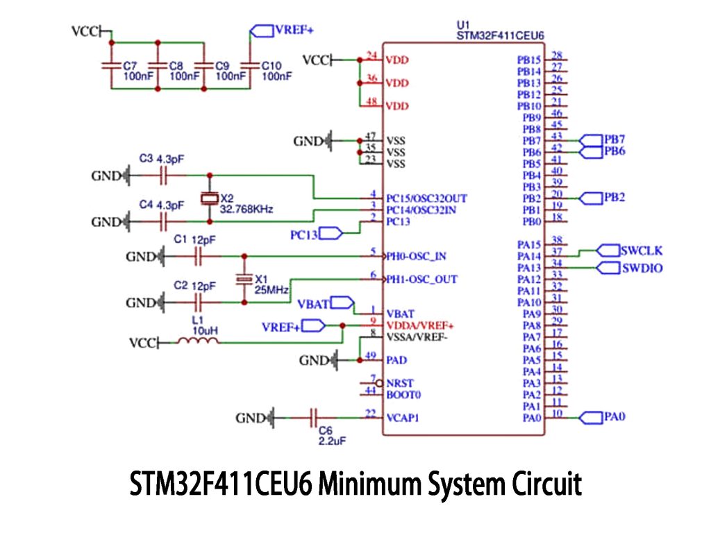
Here’s a quick look at the minimal STM32F411CEU6 circuit you’ll need for practical projects. The design is pretty straightforward, great for your prototype development. It includes decoupling capacitors at the VDD/VSS pins to ensure stable power. For the clock, a 25MHz crystal with two 12pF capacitors serves as the main oscillator, and a 32.768kHz crystal is used for the RTC. Pins like NRST (reset) and BOOT0 (boot mode) are brought out, making it easy to change startup modes. Plus, SWD debugging pins (SWDIO, SWCLK) are also included for easy connection to an ST-Link debugger—perfect for your development board setup.
STM32F411CEU6 ST-Link Programming Guide
Here’s a quick guide on flashing STM32F411CEU6 using ST-Link. Connect ST-Link’s SWDIO to PA13, SWCLK to PA14, GND to any VSS, and 3.3V to VDD. NRST is optional. Grab STM32CubeProgrammer from ST’s site or STM32CubeIDE; drivers usually install automatically. Open CubeProg, connect via ST-Link, select your firmware (.hex/.bin), hit Download, then click Run. Common issues? Ensure BOOT0 isn’t left floating, double-check SWD wiring, and verify you’re flashing to the right address (typically 0x08000000).
STM32F411CEU6 CubeIDE Project Setup
Here’s a simple guide on setting up an STM32F411CEU6 project using STM32CubeIDE. Install STM32CubeIDE, connect ST-Link (SWDIO, SWCLK, GND, VDD). Create a new STM32 project, pick STM32F411CEU6, name it, and go. In the graphical configuration, set PA9/PA10 for USART, PB6/PB7 for I2C, and choose 25MHz external crystal for 100MHz system clock. Click Generate Code, then add your code like toggling LEDs in main.c’s while loop. Click Debug to compile and flash, hit the play button, and you’re done!
Больше похожего

ISL61862HCRZ
Renesas Electronics America Inc

ISL61863GIRZ
Renesas Electronics America Inc
ISL61862GIRZ-T
Renesas Electronics America Inc
ISL61863CIRZ-T
Renesas Electronics America Inc
ISL61863KCRZ-T
Renesas Electronics America Inc
ISL61863KCRZ
Renesas Electronics America Inc
ISL61863FCRZ-T
Renesas Electronics America Inc
ISL61863JIRZ-T
Renesas Electronics America Inc
ISL61863BIRZ-T
Renesas Electronics America Inc
ISL61863EIRZ-T
Renesas Electronics America Inc
ISL61863JCRZ-T
Renesas Electronics America Inc
ISL61863BIRZ
Renesas Electronics America Inc
Также добавить в корзину

TAS5613PHD
Техасские инструменты

MPC8358VRAGDGA
Фрискейл Полупроводник

CY7C4245-25JC
Cypress Semiconductor Corp

MC100ELT25DTG
онсеми

MC74ACT373DWG
онсеми

MXDLN16G
Макссенд

TPS61100RGER
Техасские инструменты

1338C-31SRI8
Renesas Electronics America Inc

LM8500HVA9
Национальный полупроводник
MCIMX280CVM4B
Фрискейл Полупроводник

FDC6330L
онсеми

TLV2242IDR
Техасские инструменты
Сопутствующие товары
ISL61862HCRZ
Renesas Electronics America Inc
ISL61863GIRZ
Renesas Electronics America Inc
ISL61862GIRZ-T
Renesas Electronics America Inc
ISL61863CIRZ-T
Renesas Electronics America Inc
ISL61863KCRZ-T
Renesas Electronics America Inc
ISL61863KCRZ
Renesas Electronics America Inc
ISL61863FCRZ-T
Renesas Electronics America Inc
ISL61863JIRZ-T
Renesas Electronics America Inc
ISL61863BIRZ-T
Renesas Electronics America Inc
ISL61863EIRZ-T
Renesas Electronics America Inc
ISL61863JCRZ-T
Renesas Electronics America Inc
ISL61863BIRZ
Renesas Electronics America Inc
ISL61863JCRZ
Renesas Electronics America Inc
ISL61863BCRZ-T
Renesas Electronics America Inc
ISL61863ECRZ-T
Renesas Electronics America Inc
ISL61863ECRZ
Renesas Electronics America Inc
ISL61863DIRZ-T
Renesas Electronics America Inc
ISL61863BCRZ
Renesas Electronics America Inc
ISL61863ICRZ-T
Renesas Electronics America Inc
ISL61863ICRZ
Renesas Electronics America Inc
ISL61863ACRZ-T
Renesas Electronics America Inc
ISL61863HIRZ-T
Renesas Electronics America Inc
ISL61863ACRZ
Renesas Electronics America Inc
ISL61863HIRZ
Renesas Electronics America Inc
ISL61862HIRZ-T
Renesas Electronics America Inc
ISL61863HCRZ-T
Renesas Electronics America Inc
ISL61862HIRZ
Renesas Electronics America Inc
ISL61863HCRZ
Renesas Electronics America Inc
ISL61862HCRZ-T
Renesas Electronics America Inc
ISL61863GIRZ-T
Renesas Electronics America Inc
Пожалуйста, отправьте запрос предложения, мы ответим немедленно.

Пожалуйста, отправьте запрос предложения, мы ответим немедленно.
Авторские права © 2024 Все права защищены