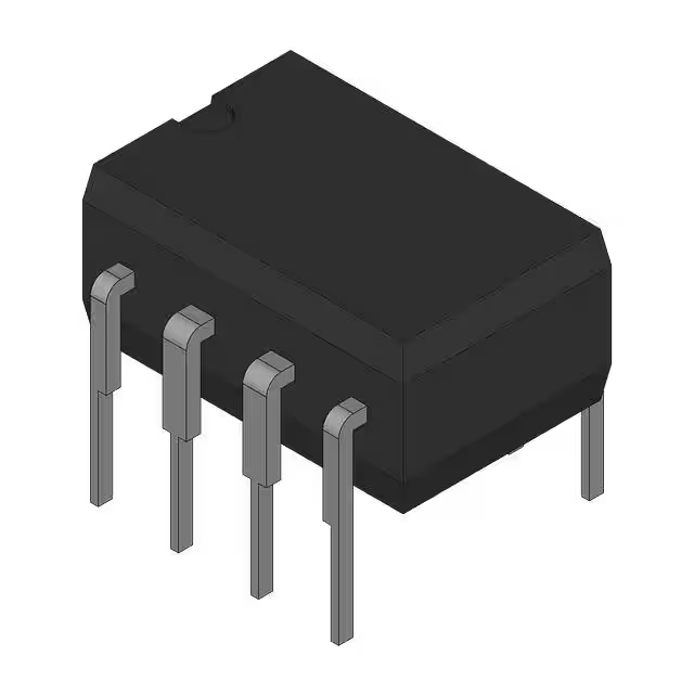
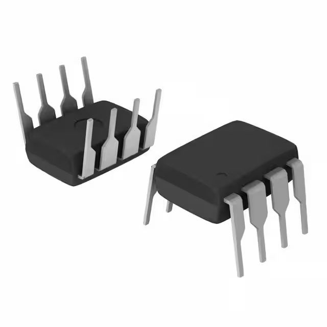
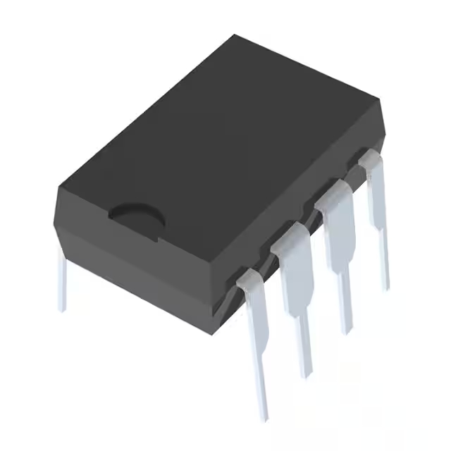
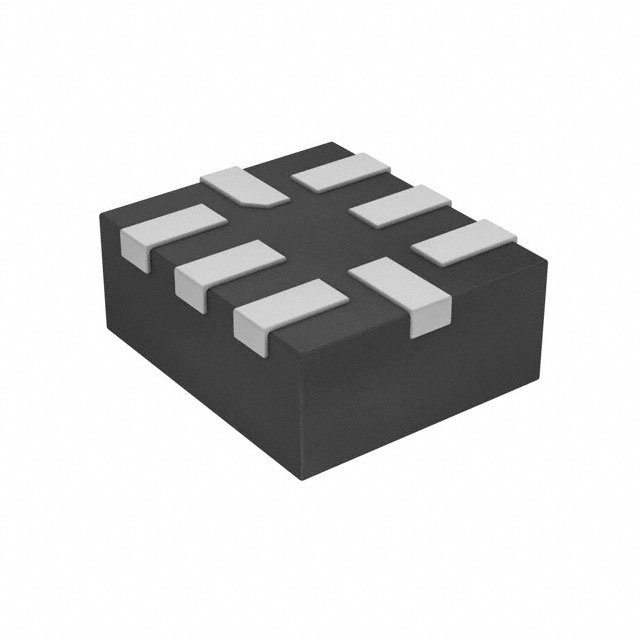
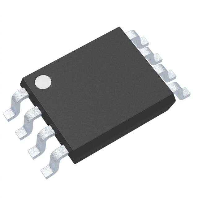
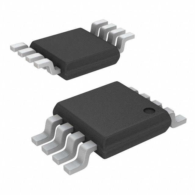
NE5532P datasheet & pdf | pinout, equivalent
- 擴大機類型: 一般
- 電路數量: 2
- 輸出類型: -
- 包裹: 8-DIP(0.300,7.62毫米)

訂單滿 HK$250.00 即可享有免運

快速回應,快速報價

閃電出貨,售後無憂

原廠通路,正品保證
Key Features of the NE5532P Op-Amp
The NE5532P is a high-performance dual operational amplifier designed for audio and signal processing applications. With a low noise level and high gain, it delivers crystal-clear amplification, making it ideal for professional audio equipment, mixing consoles, and preamp circuits. The NE5532P operates with a wide voltage range, typically 10V to 36V, and provides excellent linearity and stability. Its low harmonic distortion and high slew rate make it a top choice for applications requiring accurate and distortion-free signal amplification. Whether you’re working on audio projects or precision analog circuits, the NE5532P is a reliable and efficient choice.
NE5532P Pinout
| 別針 | Label | 描述 |
|---|---|---|
| 1 | Offset Null | Used for offset voltage adjustment to reduce offset errors. |
| 2 | Inverting Input (A) | The negative input for op-amp A (signal input). |
| 3 | Non-Inverting Input (A) | The positive input for op-amp A (signal input). |
| 4 | V- | Negative power supply pin. |
| 5 | Offset Null | Used for offset voltage adjustment for op-amp B. |
| 6 | Inverting Input (B) | The negative input for op-amp B (signal input). |
| 7 | Non-Inverting Input (B) | The positive input for op-amp B (signal input). |
| 8 | V+ | Positive power supply pin. |
Using the NE5532P Pinout
To use the NE5532P op-amp, connect your input signals to the Inverting Input (Pins 2 and 6) and Non-Inverting Input (Pins 3 and 7) depending on your desired configuration. The V+ (Pin 8) and V- (Pin 4) pins are used for powering the op-amp; ensure these are connected to a suitable dual power supply. If needed, you can adjust the offset voltage by using the Offset Null pins (Pins 1 and 5). Make sure the voltage supplied is within the recommended range to avoid damaging the IC and ensure proper performance.
NE5532P Equivalent Models
Here’s a comparison of equivalent operational amplifiers with similar packaging and features:
| 模型 | Voltage Range | 斜率 | Current Output | 封裝類型 | Noise Density | Gain Bandwidth |
|---|---|---|---|---|---|---|
| NE5532P | ±10V to ±18V | 0.3V/µs | 8毫安 | Dual In-Line | 5nV/√Hz | 10兆赫 |
| TL072 | ±3V to ±18V | 0.3V/µs | 3mA | Dual In-Line | 5nV/√Hz | 3MHz |
| LF353 | ±3V to ±18V | 0.3V/µs | 3mA | Dual In-Line | 5nV/√Hz | 3MHz |
| OPA2134 | ±2.5V to ±18V | 0.8V/µs | 8毫安 | SOIC-8 | 1nV/√Hz | 8MHz |
Substitution Tips
When replacing the NE5532P, check that the voltage range, slew rate, 和 current output match your application requirements. For instance, the TL072 和 LF353 are solid alternatives with similar noise performance and packaging but a lower slew rate and current output, which may affect performance in high-speed circuits. If you need a higher slew rate or better noise characteristics, the OPA2134 is a great alternative with a higher performance at the expense of being in a smaller SOIC-8 package. Always consider the gain bandwidth and ensure the new op-amp meets your circuit’s requirements.
NE5532P Op-Amp Overview
這 NE5532P is a reliable and versatile dual operational amplifier, perfect for audio applications and precision signal processing. It offers low noise and high performance, making it a top choice for high-quality audio equipment, mixers, and preamps. With a wide voltage range and good current output, it’s suitable for both professional and consumer-grade designs. If you need a replacement, models like the TL072 和 LF353 provide similar performance but may have lower slew rates. For higher-speed applications, the OPA2134 offers improved performance, though it comes in a smaller package. Make sure to check the specific needs of your project to pick the best alternative.
NE5532P Op-Amp Circuit Overview
這 NE5532P is a dual low-noise operational amplifier widely used in audio applications due to its excellent performance characteristics. It offers high gain, low distortion, and low noise, making it ideal for preamplifier, tone control, and audio amplifier circuits.
Circuit Diagram
Circuit Analysis
In this typical application circuit:
-
電源供應: The NE5532P operates with a dual power supply, typically ±15V, providing the necessary voltage for proper operation.
-
Input Capacitor (C1): A capacitor is placed at the input to block any DC offset and allow only AC signals to pass through.
-
Resistors (R1, R2): These resistors set the gain of the amplifier. The values can be adjusted to achieve the desired amplification level.
-
Feedback Capacitor (C2): A capacitor is used in the feedback loop to stabilize the gain and bandwidth of the amplifier.
-
Output Capacitor (C3): This capacitor blocks any DC component at the output, ensuring that only the amplified AC signal is delivered to the next stage.
Important Considerations
-
Power Supply Decoupling: It’s essential to place decoupling capacitors (e.g., 100nF) close to the power supply pins of the NE5532P to reduce noise and prevent oscillations.
-
Component Selection: Choose resistors and capacitors with appropriate voltage ratings and tolerances to ensure stable operation and minimize distortion.
-
PCB Layout: Keep the signal path as short as possible and use a ground plane to reduce noise and interference.
This simple and efficient circuit is ideal for powering low-current devices like microcontrollers, sensors, and small LEDs.
