CD4052BE circuit diagram & pinout | equivalent Texas Instruments
Explore the CD4052BE Reference Manual for comprehensive details, including circuit diagrams, pinout configurations, and schematics. Understand its equivalent components and how to integrate them into your projects effectively. Access essential information to optimize the use of this versatile component.
- 開關電路: SP4T
- 導通電阻(最大值): 240Ohm
- Voltage-SupplySingle(V+): 3V ~ 20V
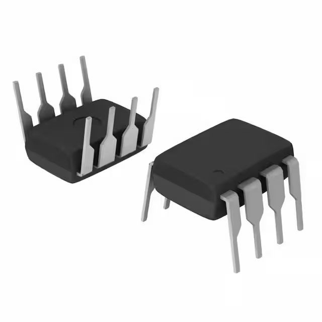
- 包裹: 16-DIP(0.300,7.62毫米)

訂單滿 HK$250.00 即可享有免運

快速回應,快速報價

閃電出貨,售後無憂

原廠通路,正品保證
PAANO MAGTEST NANG CD4052BE/ELECTRONICS GUIDE PH
CD4052BE Pinout

1:Overview of the CD4052BE:
CD4052BE is a differential 4-select 1 multiplexer, CD4052BE contains control inputs A and B, and a forbidden input.The device features low on-resistance (typically around 180Ω), low power consumption (static current less than 1µA), and a wide voltage operating range (±4.5V to ±10V dual power supply or 3V to 20V single power supply). It comes in SOIC-16 or PDIP-16 packages.
2:CD4052BE Important pin function definition:
| PIN NO. | PIN NAME | DESCRIPTION |
|---|---|---|
| 1 | Y CH 0 IN/OUT | Channel Y0 in/out |
| 2 | Y CH2 IN/OUT | Channel Y2 in/out |
| 3 | Y COM OUT/IN | Y common out/in |
| 4 | Y CH 3 IN/OUT | Channel Y3 in/out |
| 5 | Y CH 1 IN/OUT | Channel Y1 in/out |
| 6 | INH | Disables all channels. |
| 7 | VEE | Negative power input |
| 8 | 虛擬安全系統 | 地面 |
| 9 | B | Channel select B |
| 10 | 一個 | Channel select A |
| 11 | X CH3 IN/OUT | Channel X3 in/out |
| 12 | X CH 0 IN/OUT | Channel X0 in/out |
| 13 | X COM OUT/IN | X common out/in |
| 14 | X CH 1 IN/OUT | Channel in/out |
| 15 | X CH2 IN/OUT | Channel in/out |
| 16 | 電源電壓 | Positive power input |
更多類似商品
也加入購物車
相關產品
請發送 RFQ,我們將立即回覆。
版權所有 © 2024 保留所有權利


,SOT157-2.JPG)

,SOT523-1.JPG)

