
GD32F103CBT6 datasheet & price | review
- 品牌: 兆易創新北京半導體展
- 下載: -
- 價格: 詢問
- 有存貨: 9169
- 輸入/輸出數量: 37
- CPU 最大速度: 108MHz
- DAC(位元): -
- 包裹: LQFP-48(7x7)


訂單滿 HK$250.00 即可享有免運

快速回應,快速報價

閃電出貨,售後無憂

原廠通路,正品保證
Gd32f103cbt6
The GD32F103CBT6 is a 32-bit microcontroller based on the ARM Cortex-M3 core, perfect for embedded systems. Here’s a quick overview of its features:
Core & Performance: It runs at up to 72 MHz, making it ideal for real-time tasks. It has 128KB of flash storage for your program code and 20KB of SRAM for data storage and buffering.
Peripherals: It has up to 51 GPIO pins, 3 timers for PWM and signal capture, and a high-precision 32-bit timer for motor control. For communication, it includes 2 SPI, 2 I2C, and 3 UART interfaces. It also has a 12-bit ADC with 16 channels and a 12-bit DAC for audio and signal applications. Plus, it supports CAN 2.0B for industrial and automotive use.
Power & Efficiency: With a 2.6V to 3.6V operating range, it’s designed for low power consumption. It has multiple low-power modes to extend battery life.
This microcontroller is great for applications in industrial control, consumer electronics, automotive, and medical devices, offering plenty of connectivity and power management options.
Gd32f103cbt6 Pinout Reference
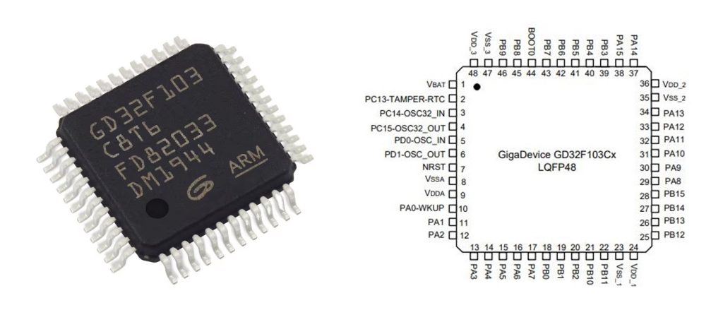
| 密碼 | 引腳名稱 | 描述 |
|---|---|---|
| 1 | 虛擬安全系統 | Power ground, connected to the power ground line. |
| 2 | 電源電壓 | Power supply, connected to 3.3V power. |
| 3 | PA0 | GPIO, multiplexed functions include ADC_IN0, USART1_RX, TMR2_CH1, etc. |
| 4 | PA1 | GPIO, multiplexed functions include ADC_IN1, USART1_TX, TMR2_CH2, etc. |
| 5 | PA2 | GPIO, multiplexed functions include ADC_IN2, USART1_CTS, TMR2_CH3, etc. |
| 6 | PA3 | GPIO, multiplexed functions include ADC_IN3, USART1_RTS, TMR2_CH4, etc. |
| 7 | PA4 | GPIO, multiplexed functions include ADC_IN4, SPI1_NSS, DAC_OUT1, etc. |
| 8 | PA5 | GPIO, multiplexed functions include ADC_IN5, SPI1_SCK, TMR2_CH1_ETR, etc. |
| 9 | PA6 | GPIO, multiplexed functions include ADC_IN6, SPI1_MISO, TMR3_CH1, etc. |
| 10 | PA7 | GPIO, multiplexed functions include ADC_IN7, SPI1_MOSI, TMR3_CH2, etc. |
| 11 | PA8 | GPIO, multiplexed functions include USART1_CK, TMR1_CH1, etc. |
| 12 | PA9 | GPIO, multiplexed functions include USART1_TX, TMR1_CH2, etc. |
| 13 | PA10 | GPIO, multiplexed functions include USART1_RX, TMR1_CH3, etc. |
| 14 | PA11 | GPIO, multiplexed functions include USART1_CTS, CAN_RX, TMR1_CH4, etc. |
| 15 | PA12 | GPIO, multiplexed functions include USART1_RTS, CAN_TX, TMR1_ETR, etc. |
| 16 | PA13 | GPIO, JTAG/SWD interface: JTMS/SWDIO |
| 17 | PA14 | GPIO, JTAG/SWD interface: JTCK/SWCLK |
| 18 | PA15 | GPIO, JTAG interface: JTDI |
| 19 | PB0 | GPIO, multiplexed functions include ADC_IN8, TMR3_CH3, DAC_OUT1, etc. |
| 20 | PB1 | GPIO, multiplexed functions include ADC_IN9, TMR3_CH4, DAC_OUT2, etc. |
| 21 | PB2 | GPIO, multiplexed functions include BOOT1, TMR2_CH3, etc. |
| 22 | PB3 | GPIO, JTAG interface: JTDO, TMR2_CH2 |
| 23 | PB4 | GPIO, JTAG interface: NJTRST, TMR3_CH1 |
| 24 | PB5 | GPIO, multiplexed functions include I2C1_SMBA, TMR3_CH2, etc. |
| 25 | PB6 | GPIO, multiplexed functions include I2C1_SCL, USART1_TX, TMR4_CH1, etc. |
| 26 | PB7 | GPIO, multiplexed functions include I2C1_SDA, USART1_RX, TMR4_CH2, etc. |
| 27 | PB8 | GPIO, multiplexed functions include TMR4_CH3, CAN_RX, etc. |
| 28 | PB9 | GPIO, multiplexed functions include TMR4_CH4, CAN_TX, etc. |
| 29 | 虛擬安全系統 | Power ground, connected to the power ground line. |
| 30 | 電源電壓 | Power supply, connected to 3.3V power. |
| 31 | PC13 | GPIO, multiplexed functions include RTC_AF1, etc. |
| 32 | PC14 | GPIO, multiplexed functions include OSC32_IN (Low-Speed External Crystal Input). |
| 33 | PC15 | GPIO, multiplexed functions include OSC32_OUT (Low-Speed External Crystal Output). |
| 34 | PD0 | GPIO, multiplexed functions include OSC_IN (High-Speed External Crystal Input). |
| 35 | PD1 | GPIO, multiplexed functions include OSC_OUT (High-Speed External Crystal Output). |
| 36 | NRST | Reset pin, used to reset the microcontroller. |
| 37 | VSSA | Analog ground, connected to the power ground line. |
| 38 | VDDA | Analog power supply, connected to 3.3V power. |
When working with the GPIO pins on the GD32F103CBT6, you have a lot of flexibility. These pins can be configured for various functions like input, output, or analog input, so make sure to set them up properly for your specific application.
Many pins also have multiplexing features, meaning they can be used for different peripherals like I2C, SPI, or USART. Just make sure the pin and peripheral are compatible when making your selection.
For things like resetting the microcontroller, the NRST pin is key. You’ll also find OSC_IN 和 OSC_OUT pins for connecting an external oscillator. Make sure your clock setup is stable for reliable operation.
這 電源電壓 和 虛擬安全系統 pins should be connected to a stable 3.3V power supply and ground, respectively. Keeping the power stable is crucial for the microcontroller to function properly.
By carefully selecting and configuring these pins, you can make the most of the GD32F103CBT6 in a wide range of embedded applications.
Gd32f103cbt6 Stm32 Compatible Alternative

| 範圍 | GD32F103CBT6 | STM32F103CBT6 | STM32F103C8T6 | STM32F030R8T6 |
|---|---|---|---|---|
| 核 | ARM Cortex-M3 | ARM Cortex-M3 | ARM Cortex-M3 | ARM Cortex-M0 |
| Clock Speed | 72 MHz | 72 MHz | 72 MHz | 48 MHz |
| Flash Size | 128 KB | 128 KB | 64 KB | 64 KB |
| SRAM Size | 20 KB | 20 KB | 20 KB | 16 千字節 |
| GPIO Pins | 51 | 51 | 51 | 37 |
| Timers | 3 × 16-bit, 1 × 32-bit | 3 × 16-bit, 1 × 32-bit | 3 × 16-bit, 1 × 32-bit | 2 × 16-bit |
| ADC通道 | 16 | 16 | 10 | 12 |
| DAC | Supports 1 channel 12-bit | Supports 1 channel 12-bit | 沒有任何 | 沒有任何 |
| SPI Interfaces | 2 | 2 | 2 | 1 |
| I2C Interfaces | 2 | 2 | 2 | 1 |
| UART Interfaces | 3 | 3 | 3 | 1 |
| 能 | Supports | Supports | 不支援 | 不支援 |
| 工作電壓 | 2.6V ~ 3.6V | 2.6V ~ 3.6V | 2.6V ~ 3.6V | 2.4V ~ 3.6V |
| 封裝類型 | LQFP-48 | LQFP-48 | LQFP-48 | LQFP-32 |
| 工作溫度 | -40℃~85℃ | -40℃~85℃ | -40℃~85℃ | -40℃~85℃ |
When choosing between the GD32F103CBT6, STM32F103CBT6, and STM32F030R8T6, here’s what you should know:
Processor Core: Both the GD32F103CBT6 and STM32F103CBT6 use the ARM Cortex-M3 core, offering more processing power for demanding applications. On the other hand, the STM32F030R8T6 uses the ARM Cortex-M0 core, which is lower in performance and better suited for simpler, resource-constrained tasks.
Storage: The GD32F103CBT6 and STM32F103CBT6 come with 128KB of Flash and 20KB of SRAM, making them suitable for mid-sized applications. The STM32F030R8T6 has just 64KB of Flash, which might not be enough for projects requiring more storage.
Peripherals: The GD32F103CBT6 and STM32F103CBT6 offer more peripheral options, including 3 UARTs, 2 SPI, and 2 I2C interfaces. The STM32F030R8T6 has fewer options, with only 1 UART and 1 SPI.
Size and Packaging: If space is tight, the STM32F030R8T6 with its LQFP-32 package is more compact, while the others use the LQFP-48, which is better for larger layouts.
CAN Support: The GD32F103CBT6 and STM32F103CBT6 support CAN for automotive or industrial communication, while the STM32F030R8T6 does not.
Gd32f103cbt6 Wiring With Usb Port
To connect the GD32F103CBT6 microcontroller to a USB port, you’ll be working with a few key pins. Here’s a simple guide:
-
USB Pin Connections:
-
D+ (Pin 12) 和 D- (Pin 11) are your data lines that connect to the USB host’s D+ and D- lines for data transfer.
-
VBUS (Pin 9) is the power line that provides 5V from the USB host if you’re powering the device through USB.
-
GND (Pin 15) connects to the ground of the USB host.
-
-
Hardware Setup:
-
Use a 100nF capacitor between VDD and GND to stabilize the power supply.
-
Place a 1.5kΩ pull-up resistor on the D+ line to ensure good signal quality.
-
-
Power Management:
-
The GD32F103CBT6 detects the USB connection via VBUS and switches to USB power mode automatically. If you’re using an external power source, you can disable the VBUS pin to save power.
-
-
Software Configuration:
-
In your firmware, configure the USB stack (like STM32’s USB library) to set up the device mode and support different USB device types, like HID or Mass Storage.
-
By following these steps, you’ll have your GD32F103CBT6 successfully connected to a USB port for communication.
Gd32f103cbt6 Pwm and Adc Usage
The GD32F103CBT6 microcontroller offers powerful PWM and ADC functionalities for your embedded projects.
PWM (Pulse Width Modulation): You can generate PWM signals using timers like TIM2. These signals are perfect for controlling motors, dimming LEDs, or other applications where you need to adjust speed or brightness. For example, you can generate PWM on the PA5 pin and adjust its duty cycle to control motor speed or LED intensity.
ADC (Analog-to-Digital Converter): The GD32F103CBT6 features a 12-bit ADC with up to 16 channels. This allows you to convert analog signals (like those from temperature or light sensors) into digital values for processing. For instance, by connecting an analog sensor to the PA0 pin, you can use the ADC to read its output and work with the data in your system.
Gd32f103cbt6 Bluepill Board Layout
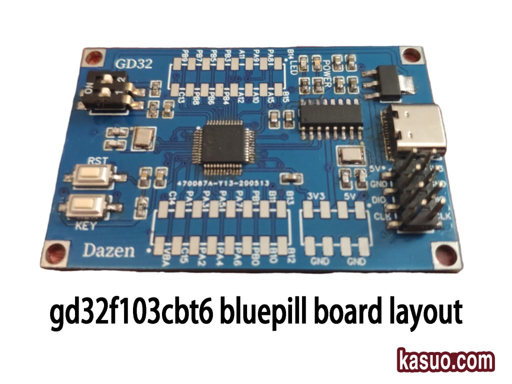
Key Components:
The main chip, the GD32F103CBT6, is powered by the ARM Cortex-M3 core, offering solid performance for your embedded applications. You’ll find 5伏 和 3.3伏 pins to power the board, with 3.3伏 being the standard. There’s also a power switch to turn the board on/off and a reset button to reboot the microcontroller if needed.
Buttons & Connectivity:
一個 user button (KEY) is available for custom functions, like triggering events. The USB port is essential for programming, data transfer, or power. For external connections, the board provides multiple GPIO pins, perfect for sensors or peripherals.
Debugging & Other Features:
There’s a small debugging header for using tools like ST-Link, and GND pins for common grounding.
Gd32f103cbt6 Programming Method
When you’re programming the GD32F103CBT6 microcontroller, you’ve got a few easy and practical options to choose from.
The best choice for most developers is using the SWD interface, connecting to tools like ST-Link or J-Link. It’s quick, simple, and great for debugging and regular code uploads during your development phase.
Another handy way is through UART ISP programming. You’ll just connect a USB-to-serial converter to the USART pins, set BOOT0 to high, and use software like GD32 ISP Programmer. This method is ideal for firmware upgrades, especially in production settings.
If you prefer simplicity in the field, try USB DFU programming—just plug into the USB port, enter DFU mode, and flash directly with DFU software.
Lastly, there’s JTAG programming, though it’s less common since SWD usually does the same job more easily.
Overall, sticking with SWD or UART will keep things straightforward and cover most of your needs.
Gd32f103cbt6 System Clock Setup
The GD32F103CBT6 microcontroller gives you plenty of flexibility when it comes to setting up the system clock. Here’s a quick rundown of how to configure it:
Clock Source:
-
HSI (High-Speed Internal): This is the default clock, running at 8 MHz, and works well for most general applications.
-
HSE (High-Speed External): If you need more precision, you can use an external crystal oscillator. It supports frequencies between 4 MHz and 16 MHz, giving you more accurate timing for sensitive applications.
PLL Configuration:
-
You can use either HSI or HSE as input to the PLL (Phase-Locked Loop) to boost the clock frequency to 72 MHz or higher (like 108 MHz) depending on your performance needs.
System Clock:
-
Set the PLL output as the system clock (SYSCLK) to get the desired higher frequency for the microcontroller.
Bus Clock:
-
AHB is typically set to match SYSCLK, while APB1 和 APB2 are configured to 1/2 or 1/1 of SYSCLK to ensure stable peripheral operation.
Flash Wait States:
-
For higher system clock frequencies, adjust the Flash wait states to ensure stable program execution.
Gd32f103cbt6 Uart Connection to Pc
To set up serial communication between the GD32F103CBT6 microcontroller and your PC, you’ll be using the USART1 interface located on pins PA9 (TX) and PA10 (RX). To make the connection, just use a USB-to-serial adapter like an FTDI or CP2102.
Hardware Setup:
-
TX (PA9): Connect this to the 接收 pin on the USB-to-serial adapter.
-
RX (PA10): Connect this to the TX pin on the adapter.
-
接地: Ensure this is connected to the ground on your PC.
Communication Process:
-
On your PC, open a serial communication tool like PuTTY 或者 Tera Term. Set the same baud rate, data bits, stop bits, 和 parity as configured on the microcontroller to ensure proper data transfer.
Use Cases:
-
This setup is commonly used for debugging, data collection, and communication between your embedded system and PC. It’s a reliable way to send or receive data during embedded development.
Gd32f103cbt6 Timer Interrupt Example
When working with timer interrupts on the GD32F103CBT6 microcontroller, you can easily set up periodic tasks like updating displays, sampling data, or controlling an LED blink. Here’s how you can configure it:
-
Enable Timer Clock: First, you need to enable the timer’s clock, such as TIM2, to get it running.
-
Configure Timer Parameters: Set the prescaler to control the timer’s frequency and the auto-reload value to determine the overflow period. For example, with a system clock of 72 MHz, a prescaler of 7199 gives a 10 kHz timer frequency, and an auto-reload value of 9999 sets the overflow to 1 second.
-
Enable Timer Interrupt: Enable the update interrupt to trigger when the timer overflows.
-
Configure Interrupts: Set the interrupt priority and enable it so the microcontroller knows to respond to the timer interrupt.
-
Start the Timer: Start the timer and let it begin counting.
-
Interrupt Service Function: In your interrupt function, clear the interrupt flag and perform tasks, like toggling an LED on a specific GPIO pin.
By following these steps, you can easily manage tasks like blinking an LED at regular intervals using timer interrupts.
更多類似商品

TPIC6C596PWG4
德州儀器
TPIC6C596PW
德州儀器

MC14557BDWR2G
安森美

74HCT595D,112
Nexperia美國公司

SN74AHC594D
德州儀器
CD4031BPWR
德州儀器
CD4035BPWR
德州儀器
CD74HCT166M
德州儀器
")
TC74HC165AP(F)
東芝半導體和存儲

SN74HC595ANSR
德州儀器

SN74LV166ADBR
德州儀器

BU4015BF-E2
羅姆半導體
也加入購物車
.jpg "7205L35J")
7205L35J
瑞薩電子美國公司

SX8676IWLTRT
Semtech 公司

MM74HC123AN-G
羅徹斯特電子有限公司

TC1303B-SI0EMFTR
微晶片技術

TW2816-TA1-GR
瑞薩電子美國公司

SIC769ACD-T1-GE3
Vishay Siliconix

SI-7510
三墾

MCP6002-I/SN
微晶片技術

PCF1179CT,112
恩智浦美國公司
SN74HC151DR
德州儀器

83052AGILFT
瑞薩電子美國公司

NXS0104BQ-Q100X
Nexperia美國公司
相關產品
TPIC6C596PWG4
德州儀器
TPIC6C596PW
德州儀器
MC14557BDWR2G
安森美
74HCT595D,112
Nexperia美國公司
SN74AHC594D
德州儀器
CD4031BPWR
德州儀器
CD4035BPWR
德州儀器
CD74HCT166M
德州儀器
TC74HC165AP(F)
東芝半導體和存儲
SN74HC595ANSR
德州儀器
SN74LV166ADBR
德州儀器
BU4015BF-E2
羅姆半導體
CD4094BPW
德州儀器
SN74LV595AQPWRQ1
德州儀器

SN74LV166ADGVR
德州儀器

CD74HC595NSR
德州儀器
SN74LV595ANSR
德州儀器
SN74LV594ADBR
德州儀器

SN74F299DWR
德州儀器
BU4021BF-E2
羅姆半導體
74AHCT164BQ-Q100X
Nexperia美國公司
74HCT597D-Q100J
Nexperia美國公司
SN74LV165APWT
德州儀器
SN74AHCT594DBR
德州儀器
74HC594D-Q100,118
Nexperia美國公司

CD74HC195NSR
德州儀器

74LVC594ABQ-Q100X
Nexperia美國公司

74AHCT164D-Q100J
Nexperia美國公司

74AHCT164PW-Q100J
Nexperia美國公司
NPIC6C596BQ-Q100,1
Nexperia美國公司
請發送 RFQ,我們將立即回覆。
