
STM32F103CBT6 datasheet | pinout & reference manual
- 核心處理器: ARM® Cortex®-M3
- 核心尺寸: 32位單核
- 週邊設備: DMA, Motor Control PWM, PDR, POR, PVD, PWM, Temp Sensor, WDT
- 包裹: 48-LQFP


訂單滿 HK$250.00 即可享有免運

快速回應,快速報價

閃電出貨,售後無憂

原廠通路,正品保證
STM32 multiple codes using class with STM32F103CBT6
stm32f103cbt6
If you’re working on embedded systems or industrial control projects, the STM32F103CBT6 microcontroller from ST might just be your perfect pick. It’s built around a powerful ARM Cortex-M3 core running at up to 72MHz, giving you plenty of speed without draining your battery too quickly.
With 128KB of flash memory and 20KB of SRAM, you’ve got enough space for your programs and data storage. It also packs useful communication interfaces like two SPI channels, two I²C channels, three USARTs, and even a USB 2.0 port for easy device connectivity.
On the analog side, there’s a versatile 12-bit ADC with up to 10 channels and an internal temperature sensor. You’ll also find multiple timers including advanced PWM timers ideal for motor control and general timing tasks.
Operating from 2.0V to 3.6V and available in a compact LQFP-48 package, it’s easy to integrate. Whether it’s industrial automation, motor control, IoT devices, or portable gadgets, this chip offers a great balance of performance, reliability, and efficiency for your designs.
stm32f103cbt6 pinout

| 密碼 | 引腳名稱 | 描述 |
|---|---|---|
| 1 | 電池電壓 | RTC and backup registers power input |
| 2 | PC13/TAMPER-RTC | GPIO or RTC tamper input |
| 3 | PC14/OSC32_IN | GPIO or 32kHz oscillator input |
| 4 | PC15/OSC32_OUT | GPIO or 32kHz oscillator output |
| 5 | PD0/OSC_IN | GPIO or High-speed crystal oscillator input |
| 6 | PD1/OSC_OUT | GPIO or High-speed crystal oscillator output |
| 7 | NRST | System reset input (active low) |
| 8 | VSSA | Analog Ground |
| 9 | VDDA | 類比電源 |
| 10 | PA0-WKUP/ADC_IN0 | GPIO or ADC Channel 0 / Wake-up input |
| 11 | PA1/ADC_IN1 | GPIO or ADC Channel 1 |
| 12 | PA2/ADC_IN2/USART2_TX | GPIO/ADC/USART2 TX |
| 13 | PA3/ADC_IN3/USART2_RX | GPIO/ADC/USART2 RX |
| 14 | PA4/ADC_IN4/SPI1_NSS | GPIO/ADC/SPI1 NSS |
| 15 | PA5/ADC_IN5/SPI1_SCK | GPIO/ADC/SPI1 Clock |
| 16 | PA6/ADC_IN6/SPI1_MISO | GPIO/ADC/SPI1 MISO |
| 17 | PA7/ADC_IN7/SPI1_MOSI | GPIO/ADC/SPI1 MOSI |
| 18 | PB0/ADC_IN8 | GPIO or ADC Channel 8 |
| 19 | PB1/ADC_IN9 | GPIO or ADC Channel 9 |
| 20 | PB2/BOOT1 | GPIO/Boot mode selection |
| 21 | PB10/I2C2_SCL/USART3_TX | GPIO/I²C2 Clock or USART3 TX |
| 22 | PB11/I2C2_SDA/USART3_RX | GPIO/I²C2 Data or USART3 RX |
| 23 | 虛擬安全系統 | Digital Ground |
| 24 | 電源電壓 | Digital Power Supply |
| 25 | PB12/SPI2_NSS | GPIO/SPI2 NSS |
| 26 | PB13/SPI2_SCK | GPIO/SPI2 Clock |
| 27 | PB14/SPI2_MISO | GPIO/SPI2 MISO |
| 28 | PB15/SPI2_MOSI | GPIO/SPI2 MOSI |
| 29 | PA8/USART1_CK | GPIO or USART1 Clock |
| 30 | PA9/USART1_TX | GPIO or USART1 TX |
| 31 | PA10/USART1_RX | GPIO or USART1 RX |
| 32 | PA11/USB_DM | GPIO or USB Data Minus |
| 33 | PA12/USB_DP | GPIO or USB Data Plus |
| 34 | PA13/JTMS/SWDIO | JTAG/SWD Data I/O |
| 35 | 虛擬安全系統 | Digital Ground |
| 36 | 電源電壓 | Digital Power Supply |
| 37 | PA14/JTCK/SWCLK | JTAG/SWD Clock |
| 38 | PA15/JTDI | GPIO/JTAG Data Input |
| 39 | PB3/JTDO/TRACESWO | GPIO/JTAG Data Output/SWO Output |
| 40 | PB4/NJTRST | GPIO/JTAG Reset |
| 41 | PB5/I2C1_SMBA | GPIO or I²C1 SMBus Alert |
| 42 | PB6/I2C1_SCL | GPIO or I²C1 Clock |
| 43 | PB7/I2C1_SDA | GPIO or I²C1 Data |
| 44 | BOOT0 | Boot mode selection |
| 45 | PB8/CAN_RX | GPIO or CAN RX |
| 46 | PB9/CAN_TX | GPIO or CAN TX |
| 47 | 虛擬安全系統 | Digital Ground |
| 48 | 電源電壓 | Digital Power Supply |
When setting up your STM32F103CBT6 microcontroller, make sure you power it from a steady 3.3V supply. Place decoupling capacitors (typically 0.1µF and 10µF) as close to the VDD and VDDA pins as possible to keep noise out. For the analog section (VDDA), use separate filtering to improve the accuracy of your ADC readings.
Your oscillator lines (OSC_IN, OSC_OUT) should be short, tidy, and away from noisy digital signals. Choose suitable load capacitors to ensure your clock stays stable and accurate.
The BOOT0 and BOOT1 pins set your startup mode—usually, tie BOOT0 directly to ground for regular use, and ground or leave BOOT1 floating (but grounding it is safer). Double-check the chip’s manual for more boot mode details.
For programming and debugging, SWD interface (SWCLK, SWDIO) is your best choice—it’s simpler and saves pins.
Finally, unused GPIO pins are best set as analog inputs or left floating. That prevents unnecessary power draw and interference, keeping your circuit reliable.
stm32f103cbt6 equivalent mcu
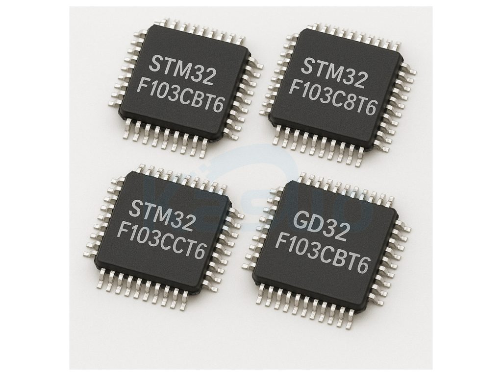
| Parameter / Model | STM32F103CBT6 | STM32F103C8T6 | STM32F103CCT6 | GD32F103CBT6 |
|---|---|---|---|---|
| 核 | ARM Cortex-M3 | ARM Cortex-M3 | ARM Cortex-M3 | ARM Cortex-M3 |
| Operating Frequency | 72 MHz | 72 MHz | 72 MHz | 108 MHz |
| Flash Memory Capacity | 128 KB | 64 KB | 256 KB | 128 KB |
| SRAM容量 | 20 KB | 20 KB | 48 KB | 20 KB |
| ADC通道 | 10 channels | 10 channels | 10 channels | 10 channels |
| GPIO (max) | 37 | 37 | 37 | 37 |
| USART Interfaces | 3 | 3 | 3 | 3 |
| SPI Interfaces | 2 | 2 | 2 | 2 |
| I²C Interfaces | 2 | 2 | 2 | 2 |
| USB Interface | USB 2.0 FS | USB 2.0 FS | USB 2.0 FS | USB 2.0 FS |
| 包裹 | LQFP-48 | LQFP-48 | LQFP-48 | LQFP-48 |
| 工作電壓 | 2.0 ~ 3.6 V | 2.0 ~ 3.6 V | 2.0 ~ 3.6 V | 2.6 ~ 3.6 V |
| 工作溫度 | -40~85℃ | -40~85℃ | -40~85℃ | -40~85℃ |
If you’re looking at alternative chips to replace your STM32F103CBT6, here’s some practical advice to keep things smooth.
這 STM32F103C8T6 has less flash memory (only 64KB), so make sure your code fits comfortably; it’s perfect for smaller or simplified projects.
On the other hand, the STM32F103CCT6 gives you a bigger flash (256KB) and SRAM (48KB). It’s pin-compatible but pricier, ideal if you need extra storage or advanced features.
Then there’s the GD32F103CBT6, a popular alternative from GD. It actually runs a bit faster (108MHz), providing a slight performance boost. Compatibility is generally good, but be prepared for some minor adjustments—especially in your clock settings and peripheral configurations—to ensure everything runs smoothly.
Whichever you pick, double-check your project’s memory needs, budget, and compatibility to avoid any surprises later on.
stm32f103cbt6 minimum system circuit

Let me walk you through the STM32F103CBT6 minimal system circuit so you can quickly understand and build your own setup:
First, you’ll want a stable 3.3V supply for the chip—just connect VDDA and VDD pins to this power source and use a few capacitors to smooth things out. Make sure you ground the VSSA and VSS pins together for stability.
Next up, the clock circuit. Grab an 8MHz crystal, and hook it to the OSC_IN and OSC_OUT pins. Place two small 22pF capacitors from each crystal pin to ground to keep the signal steady and reliable.
For resetting the chip easily, add a reset button connected to the NRST pin along with a resistor and capacitor to help stabilize this reset function—press the button, and the microcontroller resets immediately.
Don’t forget the SWD debug interface, which includes SWDIO and SWCLK pins—perfect for quickly uploading firmware and debugging your program.
Finally, you have lots of GPIO pins like PB, PC, and PA ports for sensors or external devices. PC13-15 can also handle real-time clock functions if needed.
This setup covers all your basics clearly, making your development smoother.
stm32f103cbt6 vs stm32f103c8t6 comparison
| Parameter/Model | STM32F103CBT6 | STM32F103C8T6 |
|---|---|---|
| CPU Core | ARM Cortex-M3 | ARM Cortex-M3 |
| Main Frequency | 72 MHz | 72 MHz |
| 快閃記憶體 | 128 KB | 64 KB |
| SRAM容量 | 20 KB | 20 KB |
| GPIO Pins (max) | 37 | 37 |
| ADC通道 | 10 channels | 10 channels |
| USART Interfaces | 3 | 3 |
| SPI Interfaces | 2 | 2 |
| I²C Interfaces | 2 | 2 |
| USB Interface | USB 2.0 Full Speed (Device Mode) | USB 2.0 Full Speed (Device Mode) |
| Timer Count | 3 General, 1 Advanced | 3 General, 1 Advanced |
| 包裹 | LQFP-48 | LQFP-48 |
| 工作電壓範圍 | 2.0~3.6 V | 2.0~3.6 V |
| 工作溫度範圍 | -40°C 至 +85°C | -40°C 至 +85°C |
Let me quickly break down the differences between STM32F103CBT6 and STM32F103C8T6, so you can decide which one fits your needs best.
The main difference is in the Flash memory. The STM32F103CBT6 has double the Flash (128KB) compared to the STM32F103C8T6’s 64KB. So, if your project grows and you find yourself needing extra storage for a larger program, upgrading to the CBT6 gives you more breathing room.
Apart from the Flash size, they’re basically identical. Both have the same core, frequency, SRAM, pin count, and interfaces. Plus, they’re pin-to-pin compatible since both use the LQFP-48 package, making them easy to swap out.
If you’re upgrading from the C8T6 to CBT6, you won’t have to change a thing—just drop it in and enjoy the extra space. But if you’re going the other way, from CBT6 down to C8T6, make sure your code fits within 64KB to avoid issues.
stm32f103cbt6 bootloader setup tutorial
Let’s quickly talk about Bootloaders, specifically for your STM32F103CBT6. A Bootloader is like a tiny piece of software in your microcontroller that helps you easily update firmware or manage how your application starts up. STM32 chips usually come with an official built-in Bootloader, but you can also make your own.
The STM32F103CBT6 has three boot modes set by the BOOT0 and BOOT1 pins. Usually, you’ll tie BOOT0 to ground for normal operation. If you want to flash a new program using the official Bootloader through UART, set BOOT0 to 3.3V and BOOT1 to ground. Connect PA9 and PA10 to a USB-to-TTL adapter, and use STM32CubeProgrammer software at 115200 baud to upload your firmware.
If you’re thinking about more advanced features—like OTA updates or secure firmware checks—then creating a custom Bootloader makes sense. Just carefully organize your Flash memory layout so the Bootloader and main app don’t overlap.
Always double-check your BOOT0 wiring, and make sure your USART pins aren’t already used elsewhere.
stm32f103cbt6 uart spi i2c examples
Let’s quickly talk about UART, SPI, and I²C on your STM32F103 so you can get started easily.
UART is great for basic serial communication. You just need two pins: PA9 (TX) to send data, and PA10 (RX) to receive it. Set your baud rate to 115200 for reliable data transfer.
SPI is ideal for fast communication with sensors or devices like displays. You’ll use four pins: PA5 (clock), PA6 (MISO), PA7 (MOSI), and PA4 (chip select, NSS). Make sure you manually set NSS low before sending data, then bring it high afterward.
I²C works well for sensors that need fewer wires. Connect PB6 (clock) and PB7 (data) with external 4.7kΩ pull-up resistors. Remember, I²C uses device addresses to manage communication, so always double-check these.
When using STM32CubeMX, it automatically sets your GPIO pins correctly, making setup even simpler. Just keep an eye on things like pull-up resistors for I²C and manual control of NSS in SPI to avoid confusion.
更多類似商品

BA82904YF-CE2
羅姆半導體

TSH310ILT
意法半導體

OPA374AIDR
德州儀器
OPA373AIDR
德州儀器

BU7411G-TR
羅姆半導體

MCP6V86UT-E/LTY
微晶片技術

LM4565FVT-GE2
羅姆半導體
BU7421G-TR
羅姆半導體

TLV9362IDDFR
德州儀器
TSV630IQ2T
意法半導體
TSV621AILT
意法半導體

TLV342SIRUGR
德州儀器
也加入購物車

74AUP1T97GM,115
Nexperia美國公司
DF7058BP80KNV
瑞薩電子美國公司

S82750LA
英特爾

20-101-1154
Digi

S25FL512SAGMFIG10
賽普拉斯半導體公司

MCIMX6S8DVM10AB
恩智浦美國公司
CG8520AAT
賽普拉斯半導體公司

MP4561DQ-LF-Z
單晶片電力系統公司

BCM84881B0IFSBG
博通有限公司

ISL78714ANZ
瑞薩電子美國公司

GD32F450VGT6
兆易創新

XC7K160T-2FBG676I
AMD 賽靈思
相關產品
BA82904YF-CE2
羅姆半導體
TSH310ILT
意法半導體
OPA374AIDR
德州儀器
OPA373AIDR
德州儀器
BU7411G-TR
羅姆半導體
MCP6V86UT-E/LTY
微晶片技術
LM4565FVT-GE2
羅姆半導體
BU7421G-TR
羅姆半導體
TLV9362IDDFR
德州儀器
TSV630IQ2T
意法半導體
TSV621AILT
意法半導體
TLV342SIRUGR
德州儀器

TS1871AIDT
意法半導體
SA5534ADR
德州儀器

LMV721M5
德州儀器

TLV9062SIRUGR
德州儀器
TLC271BCDR
德州儀器

TS1004IT14T
Touchstone Semiconductor
BD12732FVT-GE2
羅姆半導體

INA4181A3IPWR
德州儀器

INA4181A1IPWR
德州儀器

NCS20092DMR2G
安森美

BU7294FV-E2
羅姆半導體

TLV9102SIDGSR
德州儀器

NJU7095V-TE1
日清紡微型設備公司

OPA2310IDGKR
德州儀器
OPA2310IDR
德州儀器

BU7487F-E2
羅姆半導體

LM4559FVJ-GE2
羅姆半導體
LM4559FVM-GTR
羅姆半導體
請發送 RFQ,我們將立即回覆。
