
TDA21472 資料表與價格 | pdf
- 工作電源電壓: -
- REACH - 高度關注物質: -
- 輸入電壓 - 最小值: -
- 包裹: -


訂單滿 HK$250.00 即可享有免運

快速回應,快速報價

閃電出貨,售後無憂

原廠通路,正品保證
TDA21472
If you’re working on server motherboards or high-end graphics cards, you’ll love the TDA21472 DrMOS power chip. It integrates both the driver and MOSFET into one package, simplifying your design significantly. With its impressive 70A current capacity, it’s perfect for powering demanding processors and GPUs. Plus, it has ultra-low losses, meaning higher efficiency and reduced cooling needs.
The TDA21472 also switches very quickly, allowing you to use smaller filter components and saving PCB space. It has robust built-in protections against short circuits, overheating, and overcurrent conditions, making your designs highly reliable. Its compact, thermally-efficient package is easy to handle even in dense circuit layouts. This chip truly shines in applications that demand high-quality and stable power delivery.
TDA21472 Pinout

| 密碼 | 引腳名稱 | 功能描述 |
|---|---|---|
| 1 | 車輛識別號碼 | Input voltage (4.25V–16V) |
| 2 | LGND | Signal ground |
| 3 | EN | Enable control, active high |
| 5,7–9,20–24,40 | PGND | Power ground, linked with low-side MOSFET current path |
| 6,41 | GATEL | Low-side MOSFET gate drive output |
| 10–19 | SW | Switch node, connects to inductor and output |
| 32 | BOOT | High-side MOSFET bootstrap capacitor connection |
| Other control/monitor | SS, FB, FLT, TEMP, etc. | Includes soft-start, feedback regulation, fault, and status outputs |
When designing circuits with the TDA21472, here are a few quick tips: Separate your high-current PGND from the signal LGND to reduce noise interference. Put a 10–100 nF capacitor right next to the BOOT pin for stable MOSFET drive voltage. Control the chip using the EN pin—low means off, and around 3.3V means on—but check the allowed voltage range. Keep the SW node paths short and use thicker copper layers to boost efficiency. Remember, the thermal pad underneath needs proper cooling with PCB thermal vias. Finally, monitor the FLT and TEMP pins—they help detect overcurrent and overheating for better protection and easier troubleshooting.
TDA21472 Equivalent

| Parameter / Model | TDA21472 | TDA21462 | TDA21490 | SiC634 |
|---|---|---|---|---|
| 包裹 | PQFN-39 DrMOS | PQFN-39 DrMOS | PQFN-39 DrMOS | PQFN-39 DrMOS |
| Continuous Current | 70 一 | 60 安 | 90 A | 50 安 |
| Input Voltage Range | 4.25–16V | ~4.25–16V | Similar | Similar |
| 保護功能 | Built-in OC/OT/UVLO etc. | Built-in protection | Built-in | Built-in |
| IVR Low Voltage Optimization | 是的 | 是的 | Lower Rds(on) | New generation SiC MOSFET |
| Deep Sleep Mode | Supported (PS3/PS4) | 支援 | 支援 | 支援 |
| Application | High-end motherboard GPU/CPU | Mainstream high-end boards | High-current cards / Servers | High-efficiency boards |
If you’re considering alternatives to the TDA21472, here are a few options:
-
TDA21462 (60A): This one is pin-compatible with the TDA21472 and can be swapped without changes to your design. However, it supports only 60A, so if your system is close to 70A, ensure it’s sufficient or consider a dual-phase setup.
-
TDA21490 (90A): With a higher current rating, this one is perfect for high-demand applications (like GPU power supplies). But it’s larger and more expensive, so you’ll need to factor in thermal management and PCB layout.
-
SiC634 (50A, Samsung): Although this DrMOS supports lower current, it uses a next-gen SiC MOSFET, offering better efficiency and lower on-resistance. If your load is under 50A, it’ll provide higher efficiency, but for higher loads, watch out for overheating and overload risks.
Summary Suggestion:
If you’re sticking with ≤70A, TDA21472 is the best choice; for lighter loads and cost-efficiency, TDA21462 works well; for higher current demands, TDA21490 is a strong replacement but watch thermal management; for efficiency and loads under 50A, SiC634 provides better performance but requires stability testing.
TDA21472 Power Stage Circuit Example
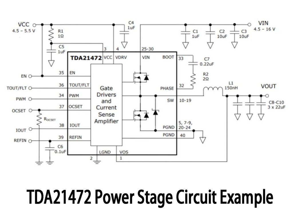
The TDA21472 chip is simple to use. The input voltage (VIN) is filtered and then converted into a stable output voltage (VOUT) via the chip’s PWM control. Inside, the MOSFETs switch based on the PWM signal, adjusting the current flow to keep the output voltage and load current stable. The OCSET pin sets the overcurrent protection threshold via an external resistor, automatically shutting down the circuit to protect against overloads. The output current sensing (IOUT) provides feedback to maintain current control.
Keep in mind that VCC and VDRV need a stable 5V voltage for the chip to work properly. The input voltage should be between 4.5V and 16V. Also, make sure to choose the right inductor (L1) to match your load requirements for efficient energy conversion.
TDA21472 Application
The TDA21472 is a high-performance power management chip designed for systems requiring efficient voltage regulation. It’s widely used in servers and high-performance computers to power CPUs, GPUs, and memory with stable, low-voltage power. It also supports multi-phase voltage regulation, improving system efficiency by reducing power loss.
With its high-frequency switching capability (up to 1.5 MHz), TDA21472 enables compact, fast-responding power designs. It’s perfect for mobile devices or embedded systems, offering low-power solutions and deep-sleep modes to save energy.
Additionally, it provides stable voltage for high-performance GPUs, ensuring system stability under heavy load. Built-in protections like overcurrent and overtemperature safeguards make it reliable for demanding power systems.
更多類似商品

TPIC6C596PWG4
德州儀器
TPIC6C596PW
德州儀器

MC14557BDWR2G
安森美

74HCT595D,112
Nexperia美國公司

SN74AHC594D
德州儀器
CD4031BPWR
德州儀器
CD4035BPWR
德州儀器
CD74HCT166M
德州儀器
")
TC74HC165AP(F)
東芝半導體和存儲

SN74HC595ANSR
德州儀器

SN74LV166ADBR
德州儀器

BU4015BF-E2
羅姆半導體
也加入購物車

MPFS025T-1FCSG325E
微晶片技術

BQ25792RQMR
德州儀器
MFR4200MAE40R
恩智浦美國公司
HPA02230AIDBVR
德州儀器
LC4032C-5T44C
萊迪思半導體公司
ZL40208LDG1
微晶片技術

ADAU1381BCPZ-RL7
ADI公司

MAX232AESE
ADI公司/Maxim Integrated

MP4581GN-Z
單晶片電力系統公司

DS90UR910QSQ/NOPB
德州儀器


ATPL100A-AZU-Y
愛特梅爾
相關產品
TPIC6C596PWG4
德州儀器
TPIC6C596PW
德州儀器
MC14557BDWR2G
安森美
74HCT595D,112
Nexperia美國公司
SN74AHC594D
德州儀器
CD4031BPWR
德州儀器
CD4035BPWR
德州儀器
CD74HCT166M
德州儀器
TC74HC165AP(F)
東芝半導體和存儲
SN74HC595ANSR
德州儀器
SN74LV166ADBR
德州儀器
BU4015BF-E2
羅姆半導體
CD4094BPW
德州儀器
SN74LV595AQPWRQ1
德州儀器

SN74LV166ADGVR
德州儀器

CD74HC595NSR
德州儀器
SN74LV595ANSR
德州儀器
SN74LV594ADBR
德州儀器

SN74F299DWR
德州儀器
BU4021BF-E2
羅姆半導體

74AHCT164BQ-Q100X
Nexperia美國公司
74HCT597D-Q100J
Nexperia美國公司
SN74LV165APWT
德州儀器
SN74AHCT594DBR
德州儀器
74HC594D-Q100,118
Nexperia美國公司

CD74HC195NSR
德州儀器

74LVC594ABQ-Q100X
Nexperia美國公司

74AHCT164D-Q100J
Nexperia美國公司

74AHCT164PW-Q100J
Nexperia美國公司
NPIC6C596BQ-Q100,1
Nexperia美國公司
請發送 RFQ,我們將立即回覆。
