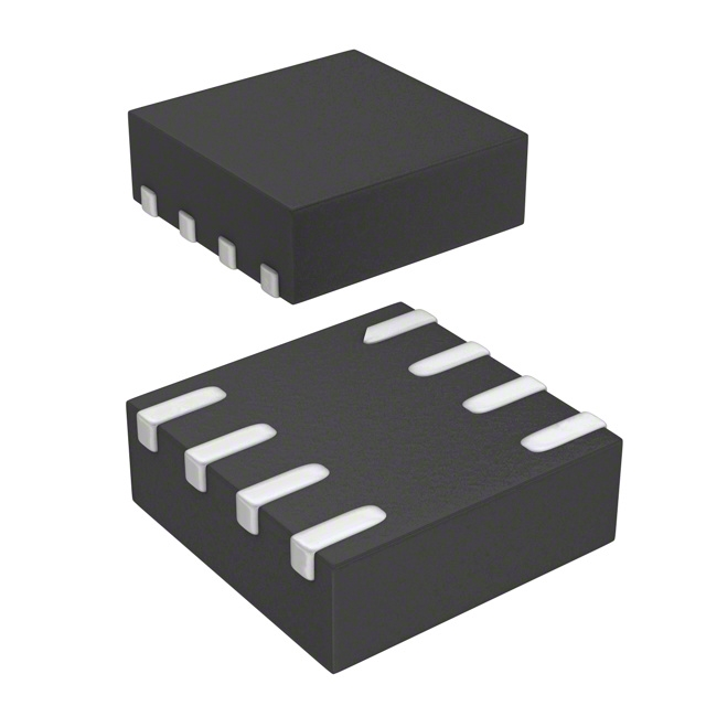
XC7Z010 數據表、價格、PDF
- 品牌: AMD/賽靈思
- 下載: -
- 價格: 詢問
- 有存貨: 28373
- L1 Cache Data Memory: 2 x 32 kB
- Number of Logic Elements: 28000 LE
- Adaptive Logic Modules - ALMs: 4400 ALM
- 包裹: -

訂單滿 HK$250.00 即可享有免運

快速回應,快速報價

閃電出貨,售後無憂

原廠通路,正品保證
Key Features of the XC7Z010 FPGA
這 XC7Z010 is a compact, powerful FPGA from Xilinx’s Zynq-7000 series, designed for embedded systems and high-performance applications. It features a dual-core ARM Cortex-A9 processor, integrated with programmable logic, allowing you to run software alongside hardware acceleration for a wide range of applications. With a 28nm process, the XC7Z010 offers low power consumption and high performance, making it suitable for everything from automotive and industrial control systems to IoT devices. The FPGA part provides customizable logic, offering the flexibility to implement complex digital circuits, while the ARM cores handle software tasks, making it a versatile choice for embedded designs. With its rich set of peripherals, including high-speed I/O, memory interfaces, and connectivity options, the XC7Z010 is a go-to solution for applications that require both programmable logic and processor-based systems.
XC7Z010 Pinout
| 別針 | Label | 描述 |
|---|---|---|
| 1 | VCCINT | Core voltage input pin, typically 1.0V. |
| 2 | 接地 | Ground pin, connected to the system ground. |
| 3 | MIO0 – MIO53 | Multi-use I/O pins, programmable for various digital functions. |
| 4 | VCCO | I/O voltage supply pin, typically 3.3V. |
| 5 | PS_MIO | Power supply pins for ARM processor system. |
| 6 | INIT_B | Initialization pin, used for configuring the FPGA. |
| 7 | DONE | Indicates when the FPGA configuration is complete. |
| 8 | GTP_RX+/RX- | Differential input pins for high-speed serial communication. |
| 9 | GTP_TX+/TX- | Differential output pins for high-speed serial communication. |
| 10 | REF_CLK | Reference clock input pin for synchronization. |
| 11 | TDI | Test Data In, used for boundary scan operations. |
| 12 | TDO | Test Data Out, used for boundary scan operations. |
Using the XC7Z010 Pinout
這 XC7Z010 has several important pins used for both power supply and digital communication. The VCCINT (Pin 1) provides power to the core logic, while the VCCO (Pin 4) powers the I/O pins. The MIO0 – MIO53 pins are multi-purpose I/O pins that can be configured for various functions like GPIO, communication protocols (I2C, SPI, UART), and more. The PS_MIO pins are dedicated to the ARM processor power and configuration. The INIT_B 和 DONE pins help with the configuration process of the FPGA. GTP_RX+/RX- 和 GTP_TX+/TX- pins are used for high-speed serial communication. Finally, the TDI 和 TDO pins are used for boundary scan and testing the FPGA. Proper power and grounding connections, along with ensuring proper I/O voltage levels, are essential for stable operation.
XC7Z010 Equivalent Models
Here’s a comparison of equivalent FPGAs with similar packaging and features:
| 模型 | Logic Cells | ARM Cores | 輸入/輸出引腳 | Clock Speed | 封裝類型 | Key Features |
|---|---|---|---|---|---|---|
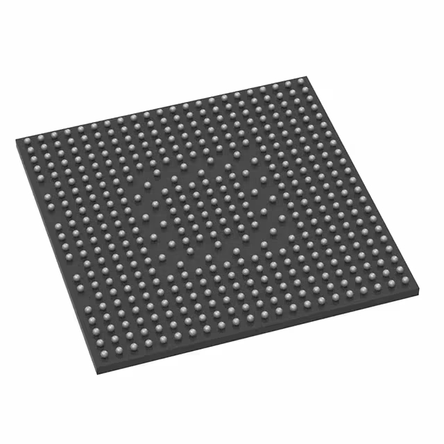
| XC7Z010 | 28K | Dual Cortex-A9 | 53 | 667 MHz | 144-ball FBGAs | Integrated ARM processor, low power, high flexibility |
| XC7Z020 | 85K | Dual Cortex-A9 | 100 | 667 MHz | 208-ball FBGAs | Higher logic capacity, same ARM cores and speed |
| XC7Z030 | 160K | Dual Cortex-A9 | 200 | 667 MHz | 484-ball FBGAs | Larger FPGA size, more I/O and processing power |
| Lattice ECP5 | 30K | – | 53 | 550 MHz | 256-ball FBGAs | Lower cost, alternative for designs without ARM cores |
Substitution Tips
When replacing the XC7Z010, pay attention to key parameters such as logic cells, ARM cores, 和 I/O pin count。 這 XC7Z020 offers more logic cells and I/O pins but maintains the same performance and ARM Cortex-A9 cores, making it a good upgrade for designs requiring more processing power. If you need a much larger FPGA, the XC7Z030 provides significantly more logic resources and I/O, ideal for complex applications. On the other hand, the Lattice ECP5 offers an alternative if you don’t need ARM cores, with a more cost-effective solution but lower clock speeds and fewer logic resources. Always check for compatibility in terms of package type 和 power supply to ensure smooth integration.
XC7Z010 Project
這 XC7Z010 is an excellent choice for building custom FPGA-based projects, especially those that require both programmable logic and a processing unit. With its dual Cortex-A9 cores and 28K logic cells, it’s perfect for embedded systems, robotics, and IoT applications. For a project, you can use the XC7Z010 to handle real-time data processing while the ARM cores run the software, offering a seamless combination of hardware acceleration and software control. Whether you’re working on a sensor interface, motor control system, or high-speed communication, the XC7Z010 can handle it all, with the added benefit of low power consumption. It’s an ideal choice for anyone looking to build a reliable and scalable solution with high flexibility.
XC7Z010 Circuit Diagram and Analysis
這 XC7Z010 is a compact yet powerful FPGA from Xilinx’s Zynq-7000 series, integrating a dual-core ARM Cortex-A9 processor with programmable logic. This integration allows for efficient handling of complex tasks, making it ideal for embedded systems, robotics, and IoT applications.
Circuit Overview
In a typical application, the XC7Z010 is connected to various peripherals and components to form a complete system. The processor system (PS) interfaces with memory modules like DDR3 SDRAM, flash storage, and external peripherals through high-speed I/O interfaces. The programmable logic (PL) section can be configured to handle specific tasks such as signal processing, communication protocols, or custom logic operations.
Key Components and Connections
-
電源: The XC7Z010 requires multiple voltage rails, including 1.0V for the core, 3.3V for I/O, and 1.8V for auxiliary components.
-
Memory Interfaces: Connections to DDR3 SDRAM and flash storage are established through dedicated memory interfaces, ensuring high-speed data access.
-
Communication Ports: Standard communication protocols such as UART, SPI, and I2C are supported, allowing for flexible connectivity with other devices.
-
JTAG Interface: The JTAG interface is used for programming and debugging the FPGA, providing a means to load configurations and troubleshoot the system.
Circuit Analysis
The integration of the ARM Cortex-A9 processor with programmable logic in the XC7Z010 allows for a heterogeneous computing environment. The processor handles general-purpose tasks and high-level control, while the programmable logic accelerates specific functions, leading to improved overall system performance. This architecture is particularly beneficial in applications requiring real-time processing, such as video processing, motor control, and sensor data acquisition.
Proper power management is crucial for the stable operation of the XC7Z010. Decoupling capacitors are placed close to power pins to filter noise and ensure clean power delivery. Additionally, careful PCB layout is necessary to minimize signal integrity issues and ensure reliable high-speed data transmission between components.
For detailed information and resources related to the XC7Z010, including datasheets, reference designs, and development tools, you can visit the official Xilinx website or consult the provided documentation.


